This thread has been locked.

If you have a related question, please click the "Ask a related question" button in the top right corner. The newly created question will be automatically linked to this question.

SN74LVC1GX04: Clock buffer is in high current state.

Part Number: SN74LVC1GX04

Hello,

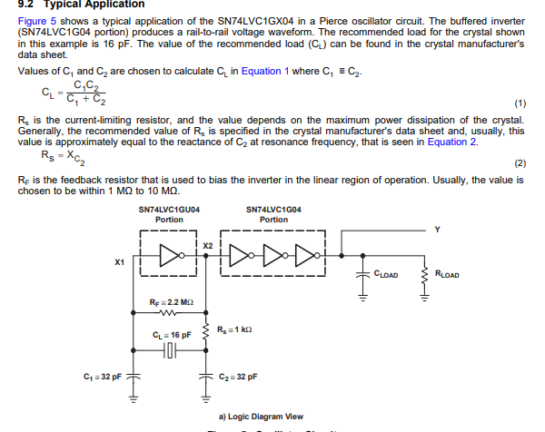
I am using the SN74LVC1GX04 to drive a clock signal in a board I am working on.  When I power on the board the SN74LVC1GX04 starts drawing a lot of current (~50mA) and heats up.  The output is not switching, either.

The oscillator I am using is the CM250C100000AZFT, found here: https://www.digikey.com/product-detail/en/citizen-finedevice-co-ltd/CM250C100000AZFT/300-8743-1-ND/2108135.

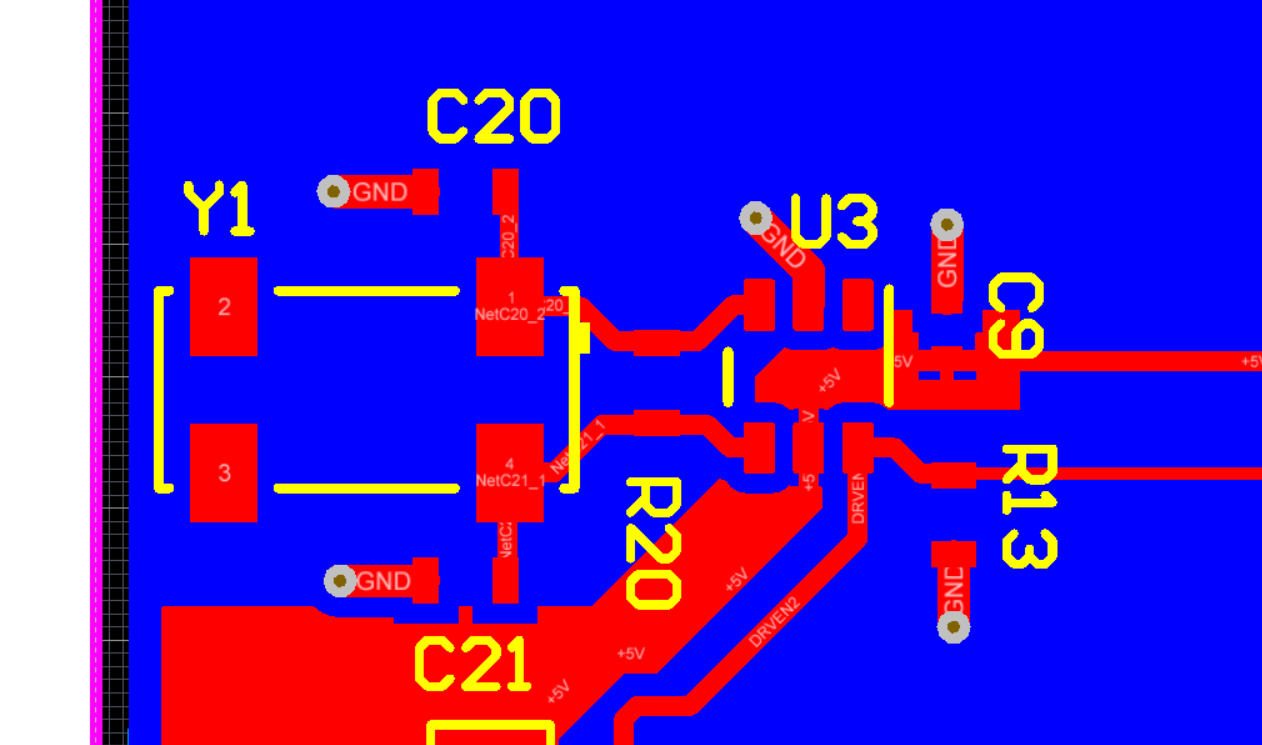
Here is my schematic snippet:

DRVEN2 goes to another IC, but I have already removed that connect to see if that improves things.  I have also added a 1kΩ resistor where I have denoted in red to see if that would limit the current.  

Any ideas?

Thanks,
Paul

  • Please show the board layout.
  • Hi Paul,
    I have a couple ideas.

    It looks to me like it would be fairly easy to reverse the oscillator and end up with pins 2 & 3 where 1 & 4 should be, or to get a short beneath it. You could also have a short at C21 to GND.

    If the LVC1GX04 has gotten very hot, I would recommend replacing it - it may have been damaged. While It's off the board, I'd check for shorts from X2 (pin 4) to GND or Vcc. The short could also be at Y (pin 6) -- I don't know what's connected on that end.
  • Hi Emrys and Clemens,

    Thanks for the response.  I believe I have found the solution for this, but I will address your comments as well for future users.

    1. Here is the layout:

    2. I have inspected the boards, and found no shorts or assembly issues.

    3.  One issue that I found interesting was that both X1 and X2 were at about 2.5V, or VCC/2.  So I started to think this was a stability issue.  The PDS describes the current limiting resistor, Rs, which I did not include in my original design.  In fact, I guess I did not pay enough attention to the apps section at all :)

    The PDS for the crystal had a Cload of 12.5pF, so I changed C20 and C21 to 27pF, to better match the recommended values.  I calculated the reactance of C21 as Xc = 1/(2pi×F×C) = 63kΩ, at the frequency of 100kHz.  My new schematic now looks like this:

    So overall, I believe the cause was not having Rs (R21).

    Thanks,

    Paul