Hi BU team
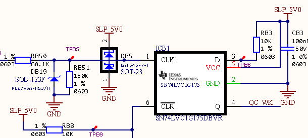
SN74LVC1G175DBVR was design in their board. The schematic is shown in below screenshot.
1. Firstly the device output a high signal at Q pin,
2. no CLK signals were input into the device.
3. power down Vcc
4. after 10s or any time, then re-powerup the device.
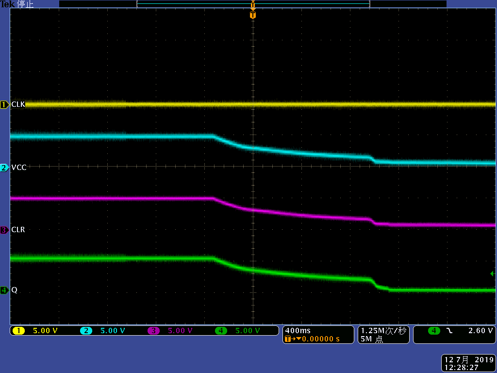
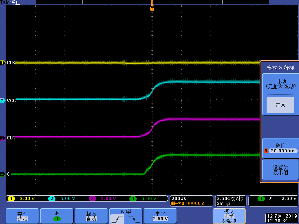
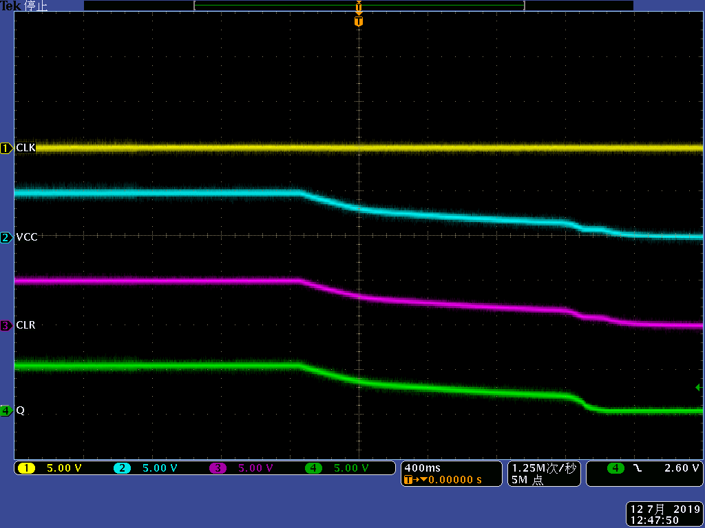
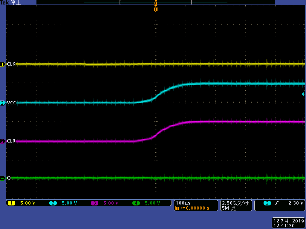
Customer found the Q output were unpredictable. Customer did the tests in 2pcs boards and captured the screenshot through scope.
Chip 1
Chip 2
Does it make sense? If customer want to get the known state at Q pin in this situation, what's your comments and solutions?
Thanks very much.


