This thread has been locked.

If you have a related question, please click the "Ask a related question" button in the top right corner. The newly created question will be automatically linked to this question.

CD40109B: Level Shifter

Part Number: CD40109B

Hello,

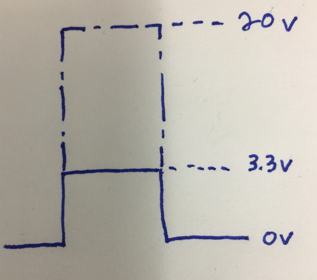
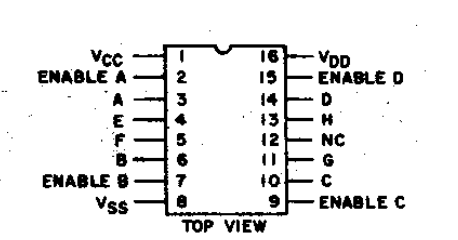
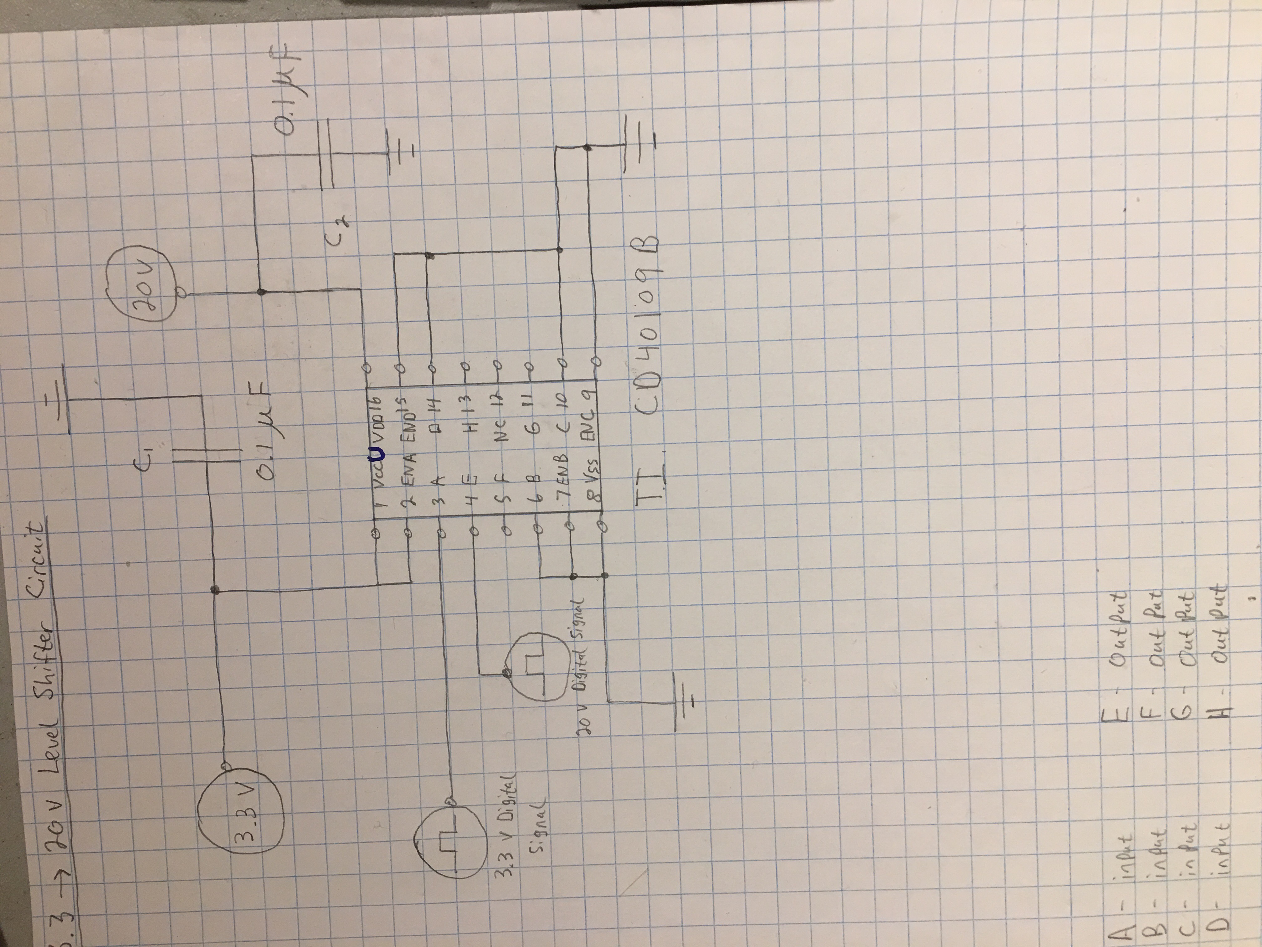
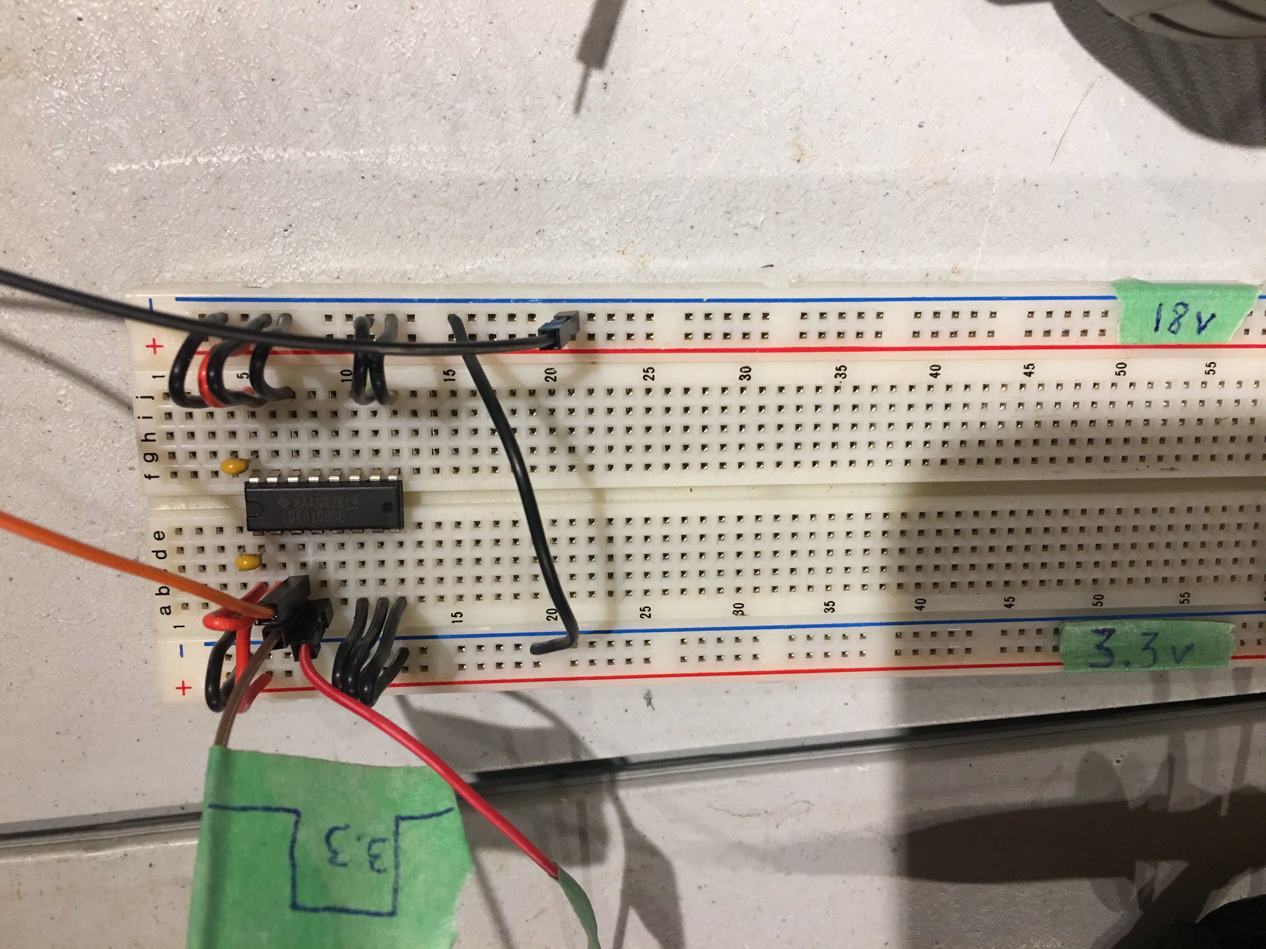
Could someone provide me a circuit diagram to make the CD40109B (or equivalent chip) level shifter to shift a 3.3V data signal to roughly 20 volts (15-20 V boost would be okay)?  I need to boost the data signal to drive it down a very long data transmission line.  I have read the technical datasheet on this chip but it is not very helpful for examples.  My data transmission speed is 115200 bps. Thanks for any help I can get. 

  • Hi,

    This is what the device looks like. You connect 3.3V supply to Vcc, 20V supply to Vdd, GND to Vss, tie all the enable pins together and connect to Vcc unless you want to disable any of the signals at any point. A, B, C, D are inputs and E, F, G, H are outputs respectively.

    Let me know if you still have questions. Remember to add decoupling caps on the supply pins.

    If you need further clarifications let me know.

    Thanks!

    -Karan

  • Hi Karan, thanks for the quick response.  Would 100 nF work for the decoupling capacitor?  

    Would this schematic be correct? Thanks so much for your help!

  • Hi,

    Firstly you will need to either tie all unused inputs (B, C, D, ENB, ENC, END) to GND or Vcc. I would recommend GND so that you disable the channels.

    100nF is the correct value for the decoupling caps. However as shown in the image you need two of them. Otherwise you are tying the supplies together which is very dangerous. Place these caps as close as you can to the device on the board.

    Thanks!

    -Karan

  • Got it, thank you so much for the help.

  • Hi Karan,

    I ordered and connected up a CD40109BE chip the exact same as the wiring schematic attached. I apply a 3.3v digital signal to Input A(3), 3.3 volt power to VCC(1), and 18V power to VDD(16) and the output signal looks identical except is only about 1.3 volts peak to peak. In the picture of my actual bread board, the left power strip is 3.3V and the right power strip is 18V. The orange wire connecting to pin 3 is 3.3V digital signal input. The brown wire right beside it runs to channel 1 of my oscilloscope. The red wire on pin 4 is output signal and connects to channel 2 of my oscilloscope. I have connected the grounds together from both my 3.3V and 18V power supplies aswell as the ground from the signal generator.

    Its probably a mistake on my behalf, something really simple you might be able to spot easily.  Wondering if you could have a look and see if there is anything obviously wrong? Thank you again for the help!   

  • Please check the voltages at all connected pins. This looks as if something is wrong with VDD.

  • Sorry, it turns out it was a problem with my oscilloscope settings. Everything is working as intended. Thanks again!