This thread has been locked.

If you have a related question, please click the "Ask a related question" button in the top right corner. The newly created question will be automatically linked to this question.

SN74LVT245B: Octal buffer seeing intermittent/latent failures where one or more channels are latching output either high or low.

Part Number: SN74LVT245B

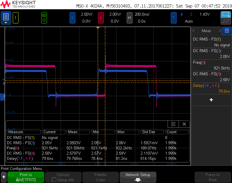
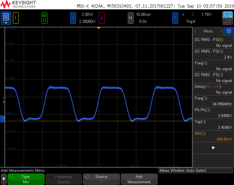
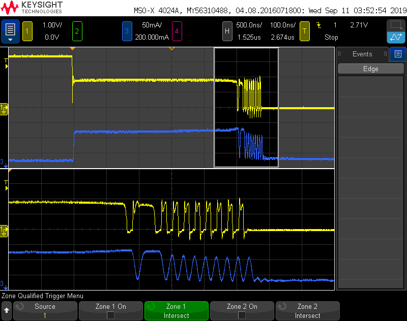
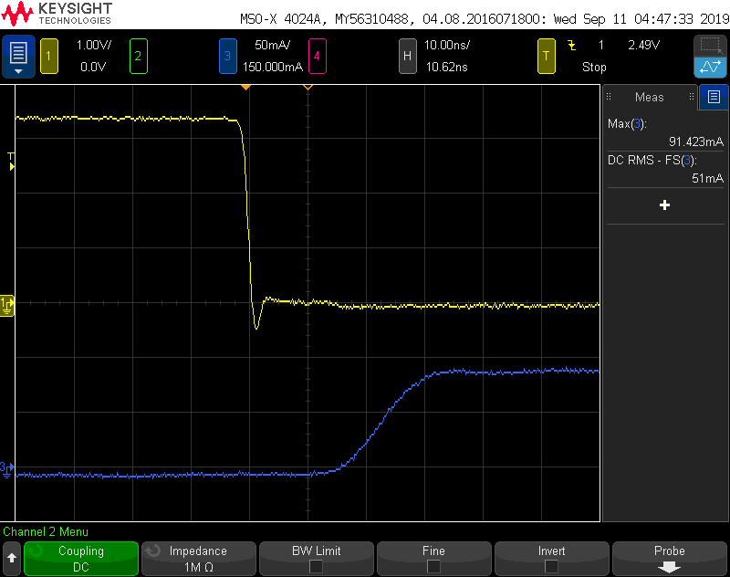
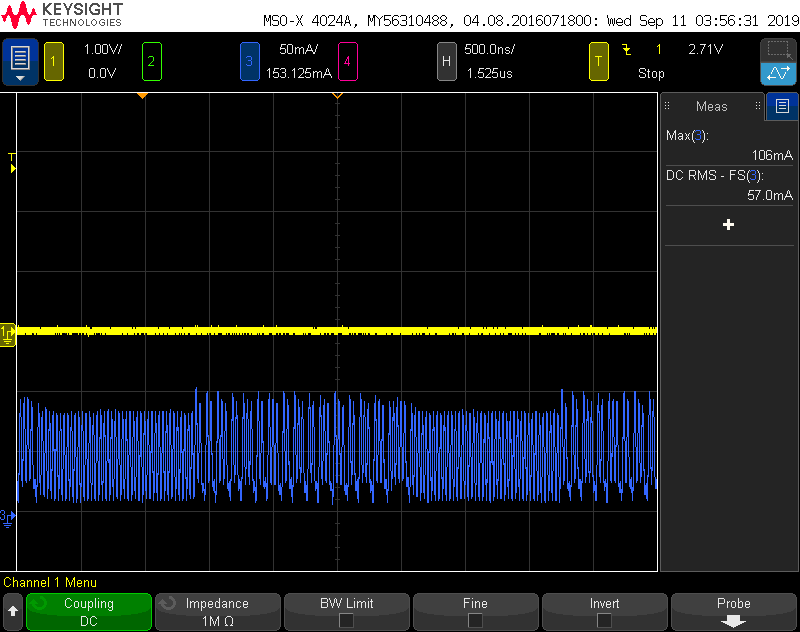
We have been using the SN74LVT245BPW to transmit switching signals ranging from 200kHz to 35MHz. The input is driven directly by a Cyclone V FPGA at 3.3V and the output drives the input of an isolator IC with 125Ω thevenin resistor terminations. SN74LVT245BPW and the isolator IC are both housed on different PCBAs. After fabrication and assembly, each PCBA with the SN74LVT245BPW component is individually tested with a fixture and all output signals are proven to work; however, after a variable amount of time in the field where both PCBAs are connected in the system, the output becomes latched to a high or a low state. The following tests have been performed with the following results:

1. Testing the individual PCBA with the SN74LVT245BPW component outside the system - output of the SN74LVT245BPW component remains latched

2. Removing the SN74LVT245BPW component from the PCBA and testing it using a bench power supply + a function generator - the output works again and input signals are transmitted at the output.

3. We have replaced the previously broken buffer with an identical new part and power cycled the system over 5000 times and have not seen the new buffer break.

See attached PDF for schematic overview of design. In the Schematic, U4 is the buffer that is failing. We would like to determine the root cause for the failure, and/or a method of early detection of the failure.

Buffer_Schematic_Overview.pdf

  • Can you show an oscilloscope trace of the I/Os (especially the output) when it's switching, in the complete system with terminated cable?

  • Hi,

    To add to the scope shots, is there a way you can measure the current into the  device supply pin during operation at 35 MHz?

  • Below is a screen capture of the 35MHz going into the bad buffer channel (Ch3 Blue) and the output pin (Ch4 Pink).

    We also tried sweeping the frequency of the input signal and saw that at lower frequencies some of the bad buffers do output, and we also see a significant delay from the time the input switches to the time the output switches. This delay looks to vary from one bad IC to another. When we replace the IC with a new one we see that the delay is around 3.5ns as specified by the datasheet. We have also observed that if you apply heat to the bad IC while it is running you see the delay will decrease.

  • Unfortunately there is no way we can measure current through the device supply pin without an intrusive or potentially destructive rework to the component on the PCBA. Is there a known specific problem in the component that the device supply current can indicate? 

  • The absolute maximum ratings forbid going more than 0.5 V beyond the rails at the outputs.

    If that horrible ringing is not a measurement artifact, and if it also happens with a working buffer, then it would explain the damage.

    Try adding source termination.

  • Hi,

    Too much current through the outputs can cause damage and so can too much current total through VCC or ground. With a heavy load and a frequency of 35 MHz, this could be a possibility. As Clemens has stated, that overshoot can also be the cause for this issue.

  • The ring is an artifact of the measurement. We were using longer ground clips when trying to measure the delay between input and output. When you measure them independently on the brand new IC with a ground spring clip you get the following.

    35MHz signal into buffer

    35MHz signal out of buffer

  • We were able to measure the current going into the VCC pin while also probing the output pins on startup, and saw that the bad pins would transition to ~1.7V, hold for a bit, then begin to oscillate, and finally latch. When making the same measurement on one of the good pins of the same IC we would not see the ~1.7V transition or oscillation and the pin would follow the input.

    Below is a shot of the output signal of the bad pin(Ch1) with the current going through VCC(Ch3)

    Below is the output signal of the good pin (Ch2) and the current going through VCC (Ch3)

    We also measured the static current when the IC was running. Below is a shot of the current going through VCC with a good IC (Ch3)

    Below is a shot of the current going through VCC with a bad IC (Ch3), there are 350KHz and 35MHz signals going into the buffers, which we believe is in the current oscillation.

  • Hi,

    I would suggest starting an FA with your distributor or dedicated sales support. this will allow us to get some of the damaged devices and run tests of our own to find a root cause of the failure.

    Currently, nothing stands out that can cause this latching issue.

  • Hi Dylan,

    I'm one of the engineers helping with this investigation. Some of the defective components have been shipped back with RAM# 60629854. Any expedited help would be appreciated.

    Regards,

    Michael

  • Hi Michael,

    The FA will allow us to get even more insight on the issue. When we receive it, I should be notified to provide support and I can provide the details given to me.

    The FA will be able to identify things I won't be able to see like ESD damage. I don't see any additional ESD protection in the schematic and being two boards with a connector, this leads me to believe there is possibilities for physical interaction. This is may not be the cause either, but the FA will help with concluding that. Unfortunately, we will have to wait until this point to keep exploring.