This thread has been locked.

If you have a related question, please click the "Ask a related question" button in the top right corner. The newly created question will be automatically linked to this question.

SN74HC164: logic level transfer error

Part Number: SN74HC164
Other Parts Discussed in Thread: SN74LVC1G17, SN74LVC1G14

Hi,

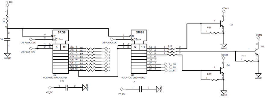
my customer's schematic is as below: U3 and U1 are two SN74HC164.

On good board, the waveform is shown below (upper picture). On bad board, the waveform is shown below(lower picture)

CH2-green. U1-PIN3: blue  U3-pin1: purple.

In theory, U1-PIN3 should be 9 clocks delayed from U3-PIN1. There should be logic high on blue line after 9clocks of logic high on purple line. But on bad board, the logic high disappear.

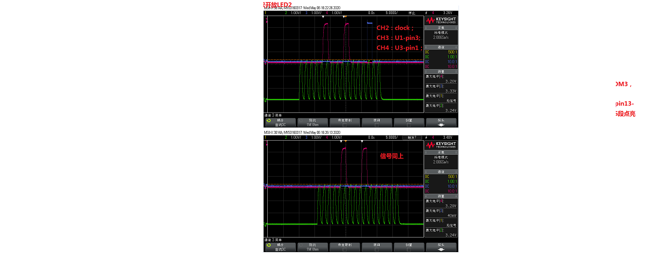
Then we measured the waveform on bad board, but now we measure U1 pin 1 instead of U1 pin3. We can see logic high on U1 pin1 after 8clocks of logic high on U3 pin1.

U1 pin1-blue, U3 pin1- purple

So it shows that the logic high on bad board is skipped from U1 pin1 to U1 pin3.

The problem happens when we use two different batches of SN74HC164 9BATHQK and 9BAECSK. If we use the same batch within 9BATHQK or 9BAECSK, there will be no problem. This device has been used for long in the customer and it's the first time we meet this problem.

Could you please suggest what to do next?

  • "The problem happens when we use two different batches of SN74HC164 9BATHQK and 9BAECSK."

    I mean U1 from 9BATHQK and U3 from 9BAECSK.

    If U1 and U3 are both from 9BATHQK, or both from 9BAECSK, there will be no problem.

  • Hi Howard,

    I would double check that the CLK signal being provided is meeting the timing requirements sections of the datasheet (7.8 - 7.10). There is a spec in the timing requirements sections that states the CLK signal be held HIGH or LOW for a minimum amount of time at a given supply voltage.

    I understand that these devices may have been working before under the given conditions, but TI does not guarantee a device's functionality when operated outside of spec given by the datasheet. A possible solution to the CLK signal operating outside of spec is using a device with Schmitt Trigger inputs.

    If you have any other questions, please don't hesitate to reach back out.

    Thanks!

    Chad Crosby

  • Chad,

    it's caused by the series connection of 2 SN74HC164 with the same clock source.

    For the second device, the clock's rising edge is simultaneous with A/B signals rising/falling edge, so the sample of the digital signal may be incorrect.

  • Hi Howard,

    Right, so if the issue really is the transition of the data and clock at the same time, does your board have space to put a buffer between U3PIN13 and U1PIN1?

    If so, the SN74LVC1G17 would be enough to buffer the output from the clock and avoid this conflict.

    Thanks!

    Chad Crosby

  • Chad,

    sorry that I don't understand why a buffer would help.

    The transition of the data and the clock should still at the same time even with the buffer added, right?

  • Hi Howard,

    The thought was to try and introduce some delay somewhere in the system to ensure that the data and clock lines are not switching at the same time. Will this work for the customer if the output signal is more delayed? The SN74HC164 has a setup time before rising clock edge specification (Section 7.8 of the datasheet) that needs to be followed in order for this device to function properly.

    Another suggestion would be to invert the clock signal to U1 to add a bit more time for this setup to happen. The SN74LVC1G14 would work for this purpose.

    Thanks!

    Chad Crosby