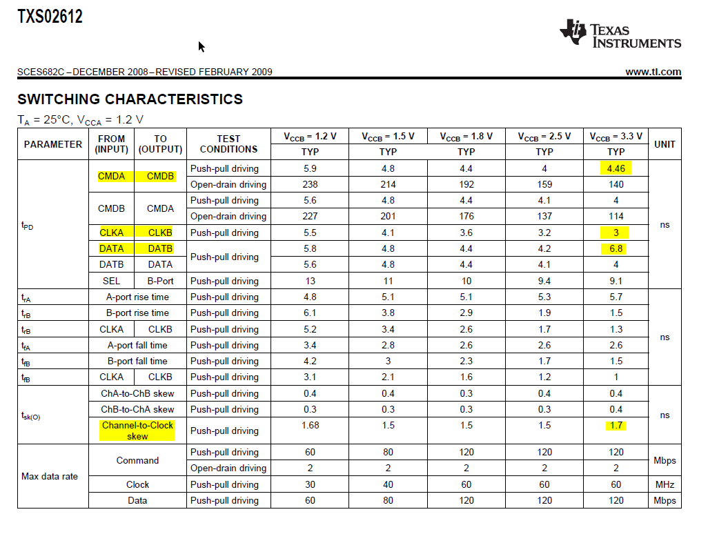
The switching characteristics table for VCCA=1.2V and VCCB=3.3V has conflicting timing parameters.
tPD (DATA to DATB) = 6.8ns
tPD (CMDA to CMDB) = 4.46ns
tPD (CLKA to CLKB) = 3.0ns
tsk (Channel-to-Clock skew) = 1.7ns
Can you please clarify how the clock and data propagation delays can vary by 3.8ns yet the channel-to-clock skew is listed as 1.7ns?