This thread has been locked.

If you have a related question, please click the "Ask a related question" button in the top right corner. The newly created question will be automatically linked to this question.

SN74AVC2T245: VCCB Is Affecting my VCCA signal SI

Part Number: SN74AVC2T245

Hi, I'm currently using SN74AVC2T245 with VCCA  = 1.8V and VCCB support voltage like 1.2V, 1.5V, 1.8V, 2.5V, 3.3V. I have attached the schematic as below:

When I drive signal from port A to port B, I noticed that the different VCCB is affecting my VCCA SI. This make no sense to me as my VCCA and VCCB are from different power source. 

From my experiment and the screenshots below, it looks like when VCCB = 3.3V, the SI at port A is the worst. While 1.2V is giving the best SI. 

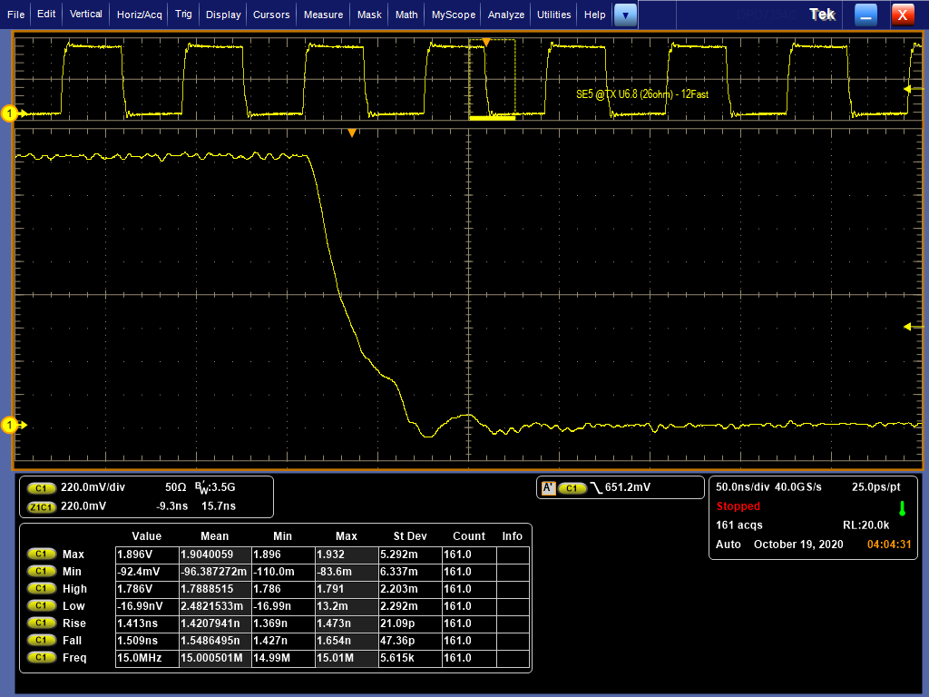
Port A Signal When VCCB = 3.3V, 

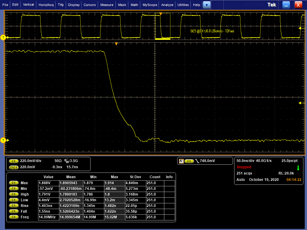
Port A Signal When VCCB = 2.5V, 

Port A Signal When VCCB = 1.8V, 

Port A Signal When VCCB = 1.2V, 

Would SN74AVC2T245 change its internal impedance when VCCB is switching, and thus affecting my SI? Else, what could be the reason?

Looking forward for the reply.

Thanks. 

-Lay Ying

  • Hey Lay,

    None of your images came through. Though, changing the supply at the output shouldn't affect the input signal.

  • Hi, sorry. Let me reattached the screenshots. 

    Schematic design as below:

    Port A Signal When VCCB = 3.3V, 

    Port A Signal When VCCB = 2.5V, 

    Port A Signal When VCCB = 1.8V, 

    Port A Signal When VCCB = 1.2V, 

    From my screenshots, you can see the SI on port A changes when I change the VCCB voltage. If it shouldn't happen, would there be any other possible reason ? Could you advice me?

    Thanks. 

    -Lay Ying

  • Hey Lay,

    What you are referring to is called ground bounce and is caused by parasitics likely from the PCB. Your bypass caps should be helping with this, are they physically close to the supply pin of the device?

    More details can be found on this if you web search ground bounce, and you can likely find methods to help reduce. The reason its more prominent when the VccB supply is higher is due to the output driver being stronger at higher supply voltages.  

  • Hi, I'm not sure whether you get my problem correctly. Perhaps let me explained again in more details. 

    My VCCA is always a constant 1.8V while VCCB could be changed. What I observed here is, when I was driving the signal from port A to port B while keeping VCCA always =1.8V,  the signal SI measured at port A is the worst when VCCB = 3.3V while the best when VCCB = 1.2V. Yes, I know, by common sense, VCCB shouldn't affect the input signal. However, I'm seeing this behaviour and doesn't have a clue why would that be. Is my design inappropriate (I have attached the schematic in previous, could you help to check?) or could the SN74AVC2T245 internal impedance change when voltage changes, and thus affecting the SI?

    By the way, the cap has been placing very close to the supply pin. I do not see it has any problem. I'm looking forward to your advice again.

    Thanks. 

    -Lay Ying 

  • CMOS inputs have a very high impedance. What changes it not any characteristic of the input, but the current through GND, which is shared by both sides.