This thread has been locked.

If you have a related question, please click the "Ask a related question" button in the top right corner. The newly created question will be automatically linked to this question.

TXB0106: SPI signal not being translated correctly

Expert 1105 points
Part Number: TXB0106

Hello,

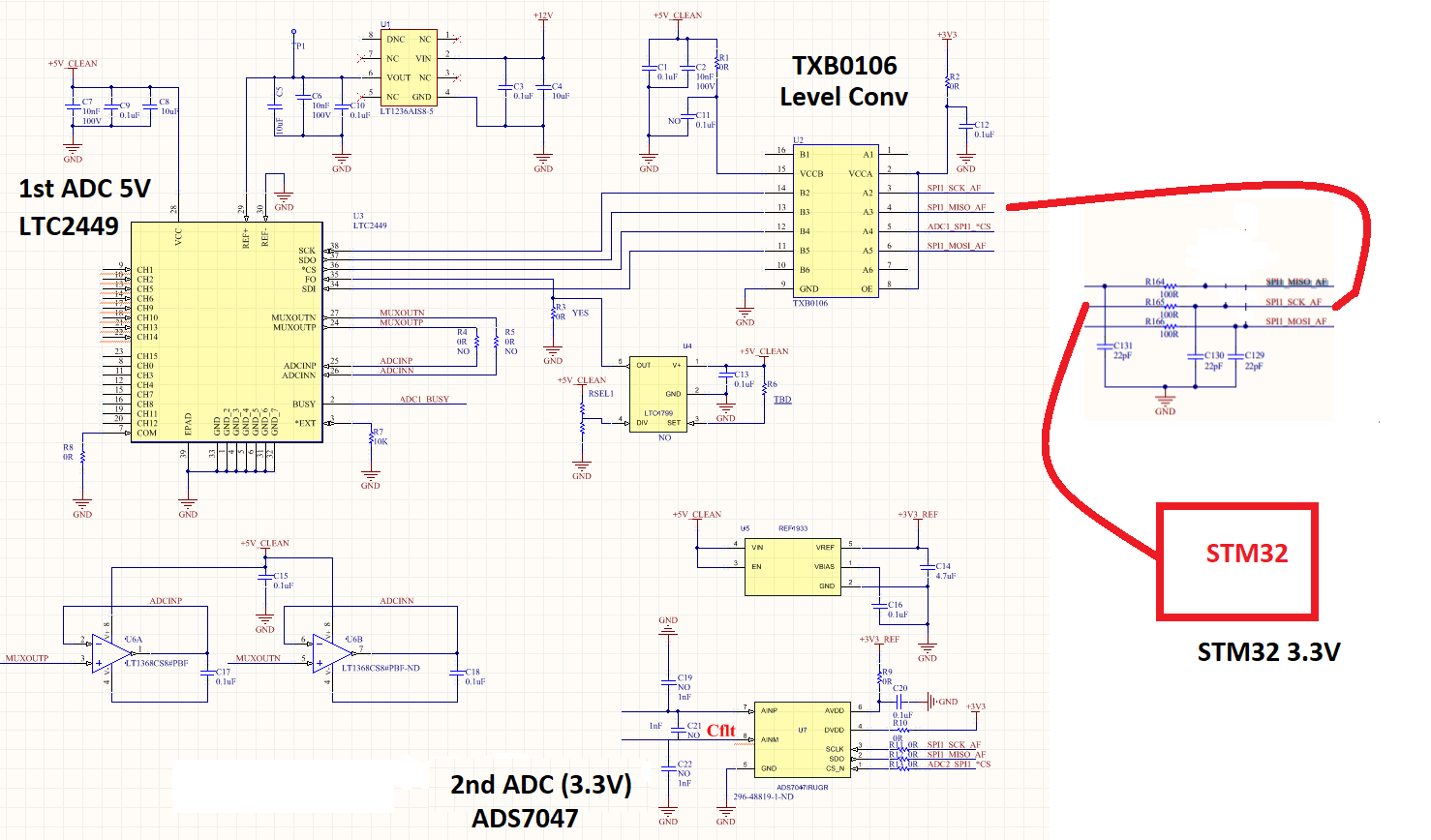
we have a system with 2 ADC and a MCU

* ADS7047  (runs at 3.3V) named as ADC 2

* LTC2449   (runs at 5V)  named as ADC1

* STM32 MCU (runs at 3.3V but is 5V tolerant)

we placed a level converter TXB0106 between ADC1 and the rest of the 3.3V side but SPI signals are not being level translated properly. Below is the schematic of the related part.

Without the level translator everything works fine (when we place a resistor divider on the MISO signal) so rest of the system is verified. We would be happy if you share your thoughts regarding this problem.

  • Hello again,

    SPI rate for the system is around 4.5 MHz.

    I forgot to mention this in my previous post.

  • Hey Rifo,

    I'm assuming the capacitive loading is too large for our device, its recommended to keep CL<70pF. External pull-ups or pull-downs should should not be used on the I/O of this device. I recommend removing any that may be connected or at least keep them larger than 50 kohm.

  • Hello,

    Thanks for the answer. We removed the filter capacitance and resistors. We also disconnected miso line of ADC 2.  Everything is connected with pcb tracks only, no other components.
    Unfortunately the system doesn't work reliably.Below you can find the screenshots.

    Below screentshot is CLK signal at stm32 side (the signal is nice)

    Below screentshot is CLK signal at ADC 1 side

    Below screenshot is MISO signal at ADC 1 side  (signal is nice)

    Below screenshot is MISO on STM32 side

    Can you please advice how we should proceed?

    Best Regards

  • Hey Rifo,

    The rounded edges of your signals still makes it apparent there is a lot of capacitance still there. How long are these traces? Are you driving the signal through a cable? If the loading was < 70pF, it wouldn't look like this.


  • Hello,

    Attached you can find a screenshot of our trial.

    The distance between TXB0106 and ADC 1 is very short.

  • Hey Rifo,

    If you are telling me your capacitive loading is indeed <70 pF and your signal still looks like that, then I would recommend swapping device with another to see if the previous was damaged in some way. 

  • Allright, will do that.

    Aside from that, can you recommend a way to measure the capacitive loading? So that we can be sure that capacitive loading  is under 70pf

  • Hey Rifo,

    They may be test equipment to do this, but an easy estimation can be done by  measuring the rise time and then back calculate the time constant (RC). This will be difficult with the current device since it has an edge rate acceleration to improve the AC drive and doesn't have a constant output impedance. If you look closely at your scope shots (you can even zoom in to get a better view) you will see the edges have a sharp edge followed by a spike and then it has a slow roll off. This is the one shot in action trying to speed up the edge. This circuitry is supposed to drive the signal to 95% or for 10 ns (whichever comes first). You can see that it times out before reaching 95%, the 4kohm series resistor is then in charge of getting the signal the rest of the way. This means you can back calculate for the RC after the one shot is done since you know R will be ~4Kohm. However, just note that the one-shot timing out is an indicator for me that the load capacitance is large or there may be some damage to the device.