Other Parts Discussed in Thread: SN74HCS595
I am trying to find out if the output pins have clamping protection to Vcc and ground.
This thread has been locked.
If you have a related question, please click the "Ask a related question" button in the top right corner. The newly created question will be automatically linked to this question.
I am trying to find out if the output pins have clamping protection to Vcc and ground.
Hey Jim,
Here's a good FAQ on this :
[FAQ] Can the input voltage (Vi) to my logic device be higher than the supply voltage (Vcc)?
In this case, the device does have the clamping diodes to VCC and Ground.
Thanks,
Rami
I am looking for information on the output structure, such as clamping devices, of the output pins, not the input pins.
Sorry about that, I highlighted the wrong thing. The answer remains the same for input and output
Thanks!
Rami
Rami,
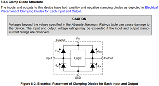
Thanks for the feedback. I believe this confirms a clamping structure on the output pins. Some of the older datasheets used to include schematic representations of the input and output pin structures, but do not see that information in more recent datasheets. I wish that information was included in the datasheets.
Regards,
Jim
Hey Jim,
I agree that this is useful information and I don't particularly like that our datasheets stopped showing this information more clearly.
Our most recent datasheet format now includes the clamp diode information again.
The new HCS (SN74HCS595) logic family uses this format: