This thread has been locked.

If you have a related question, please click the "Ask a related question" button in the top right corner. The newly created question will be automatically linked to this question.

SN74AVC4T234 input voltage

Other Parts Discussed in Thread: SN74AVC4T234

Hello,

I would like to clarify some doubts with SN74AVCT4T234

- If VrefA=2.5V and VrefB=1.8V, is it possible to input a signal with 3.3-logic to convert it to a 1.8-logic signal?

- Just to make sure I am not missing anything... to accomplish the conversion, it is only necessary to set the VrefA to the desired output voltage, no pull-up resistors are required, it's ok?

Thank you for your help

Regards

  • Thank you for your post.

    Both VCCA and VCCB can be supplied at any voltage between 0.9 V and 3.6 V. SN74AVC4T234 is suitable for translating between any of the low voltage nodes (1V, 1.2 V, 1.8 V, 2.5 V, and 3.3 V). Data rates vary by the voltage levels.

    Vcca and Vccb do not need pullups. Decoupling capacitors 0.1uF as close as possible to the pins are recommended. None of the unused I/O must be left floating.

    Thanks
  • Thank you for your answer Clarisa

    My doubt is regarding VrefB voltage and B-input voltages.If I set VrefB to 3.3V and VrefA to 1.8V, is it possible to translate 2.5V-logic input signals to 1.8V? and also with VrefB=2.5 it is possible to translate 3.3V-logic input signals? 

    The point is if input signals high voltages must match with VrefB or not. 

    The datasheet says that any unused input signal must be grounded or tied to VCCi, but nothing is said about the outputs, should I connect them to GND or Vcco?

    Thank you

    Regards

  • Hi

    A connection schematic will help. I dont see what Vref you are referring to. Whatever voltages you are connecting on Vcca and Vccb are that gets translated.

    All I/O input/output should not be left floating.

    Thanks

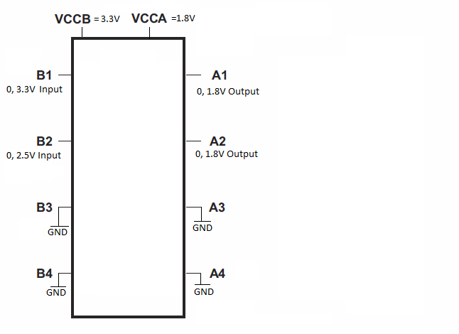
  • Sorry, VrefB and VrefA  was a mistake, I meant VccB and VccA. The doubt is represented in the following drawing, is possible this configuration?

    B3/A3 and B4/A4 are unused and B2 input signal is lower than VccB. 

    thank you!

  • Hi Jennifer,
    Could you help me with this doubt? if the drawing is not clear or you need further information please let me know.
    Thank you!

    Regards
  • The voltages you are translating are on Vccb and Vcca.

    The input ports have VIL max, Vcci*0.35 and VIH min Vcci *0.65 as shown in page 4 of the datasheet.

    Thanks