


Hello,
In Fig 1 Load Circuits and Voltage Waveforms on page 5 of the datasheet (SDAS025D, April 1982 - Revised March 2002), there are three load circuts: 1) RL from output to GND, 2) RL from output to Vcc, 3) R1 with S1 to 7V from output, and R2 from output to GND.
In our design, the output of SN74ALS541 is going to connect to the input of a TTL device. We have the following questions:
a) which load circuit should be used between the output of SN74ALS541 and the input of the TTL device: 1, or 2, or 3?
b) if the load circuit 3 is used between the two devices, could R1 connected to Vcc instead of 7V?
c) when R1 (560 ohm) is connected to Vcc, the VoH is jumping between 3.2V and 2.4V (see the attached file)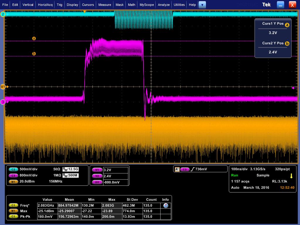 , is this the expected outcome?
d) when the load circuit 1 (RL=560 ohm) is used, the VoH is jumping between 3.2V and 2.4V (see attached file), is this the expected outcome?
e) does this device have an output damping resistor? If not, should that be ok to put a 25 ohm damping resistor between the output and the input of the next TTL device?
Best regards,
Mark Liang
