This thread has been locked.

If you have a related question, please click the "Ask a related question" button in the top right corner. The newly created question will be automatically linked to this question.

SN74LVC1G11: A few issues / questions

Part Number: SN74LVC1G11
Other Parts Discussed in Thread: SN74LVC3G17, SN74LVC1G97, SN74LVC1G99, SN74LVC1G123

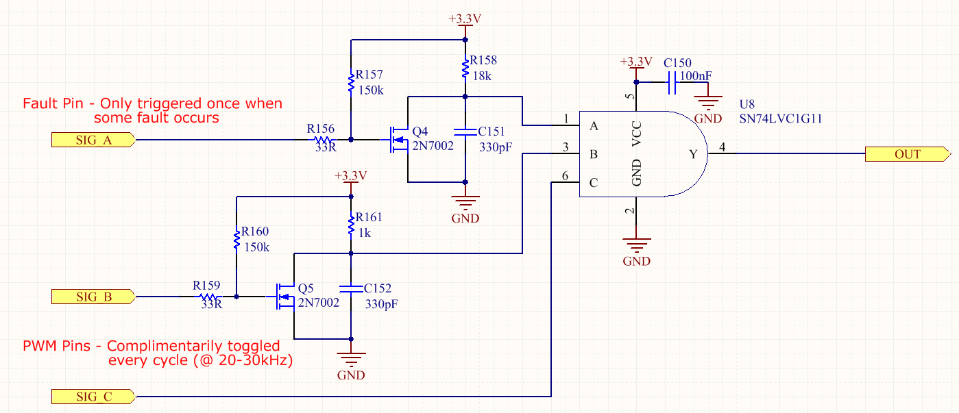
I have an application where I need to use discrete logic to control the input to a driver IC. Some of the key criteria included using only one IC in a small package and relatively low propagation delay. I chose to use the SN74LVC1G11(Single 3-Input Positive-AND Gate) to accomplish the task.

See attached simulation/schematic.

There is very specific behaviour that is required from this circuit, including some inversion and latching (for a period of time) of input signals. The circuit does exactly what I need but after I had built the first prototype, I have discovered some possible design issues (Note: Not from testing but from datasheet analysis).

I believe that both RC delay circuits on inputs A and B violate the "Δt/Δv Input transition" rating of 10ns/V. If I understand correctly with a VCC of 3.3VDC, to comply with the datasheet figures, I need to ensure the inputs transition within about 33ns from 0.8V to 2V. Is that understanding correct?

Signal B and C are toggled at 20kHz. Signal A is rarely toggled - It's a fault pin that is meant to send the output low if signal A goes high. It's designed to latch the output of the gate low for a few microsecs (kind of one shot behaviour).

Signal input C is ok - no violation. Signal B input stays between 0.8V - 2V for about 200ns while Signal A stays in transistion for several micoseconds.

Does this situation pose any real risk? I don't believe there will be any significant increase in VCC current nor will there be any additional heating. I haven't witnessed any oscilliations in testing either. I have read the app note regarding slow inputs but the paper emphasizes the risk when there are multiple gates in a single package. In this case there is only one gate and for my analysis the risk seems quite minute.

If I had to change this part, I suppose I should use a part with schmitt trigger inputs. I can't find any single 3 input AND gate with schmitt trigger inputs nor even a dual AND gate that I could cascade. Are there any other options, noting that I need single gate IC solution and prefer a low total propagation delay.

Thanks

  • Hello,

    Your schematic didn't seem to get posted if you want to repost, but I understand what is going on.

    You are correct that the rising edges need to be fast 33ns from 0 to 3.3 or 12ns from 0.8 to 2.0V. This transition rate is tested to be a guarantee of operation for the device. Technically, if you are violating the specification then we don't guarantee the operation of the device.

    If the rising edge is fast enough, and if you're not seeing oscillation and can tolerate the slightly elevated ICC, then in all likelihood the device is going to be fine, but again we can't absolutely guarantee it. 

    The major concerns are increased current consumption and oscillations as you mentioned. It would be recommended to use schmitt trigger inputs, but unfortunately we don't have a 3 input AND gate with schmitt trigger inputs. The next best option would be to use the SN74LVC3G17, but as you mentioned, you need a 1 chip solution.

    Here are a couple of app notes that might help as well, but I think for the most part you understand the concerns that are contained within these documents.

    www.ti.com.cn/.../slla364a.pdf

    http://www.ti.com/lit/an/scba004d/scba004d.pdf

    Feel free to let me know if you have additional questions or concerns.

    Best,
    Michael

  • There is no single device that does what you want.

    You could use two Schmitt-trigger AND gates (SN74LVC1G97).

    Please show the schematic; it might be possible to use three inputs of the SN74LVC1G99.
  • Not sure what happened. I'll try to upload schematic again:

  • I figured this would be the response. Thanks for the feedback. I've now uploaded the schematic properly.

    Short term, I think I can continue testing on my existing prototypes. I'll look at changing design in next iteration to include proper schmitt triggering. I'll see if one of those configurable logic gates can accomplish the same logical behaviour OR assess the impact of adding an additional schmitt buffer.

    If you have any other ideas based on the schematic, I'm open to any other more elegant suggestions.
  • Is "complimentarily" intended to be "complementarily"? And does this mean that these two signals are the inverse of each other? That would imply that SIG_C does not really have an effect and could be left out.

  • Yes, you're correct - that was a typo. I meant complementarily. BUT not exactly - The signals may or may not be exactly 180 degrees out of phase. I do need to make use of both signals due to other parts of the circuit including hardware and software.

    The desired logic is as follows:

    • OUT pin should go low immediatelyif:
      • SIG_C goes low OR
      • SIG_A goes high OR
      • SIG_B goes high
    • OUT pin should go high when:
      • SIG_C goes high AND
      • SIG_A is low and has been low for at least several microseconds AND
      • SIG_B is low and has been low for at least several hundred nanoseconds

    The FET on SIG_B could be replaced with logic but the FET on SIG_A probably needs to stay as there are multiple SIG_A type signals that feed other open-drain FETs which all connected to the same RC circuit (eg. all connect at net between R158 and C151). This pin is kind of a "catch-all" fault pin that is supposed to latch for a period of time.

    I should add that SIG_C can always transition at better than 10ns/V so doesn't need to be buffered with a schmitt device.

  • The SIG_B FET could be replaced with the SN74LVC1G123, but that would not help.

    As far as I can see, the best choice would be a Schmitt-trigger AND gate for A and B, and another AND gate to combine this with C. If SIG_B has enough drive strength to charge the capacitor, it would be possible to omit the B FET and instead configure an SN74LVC1G97 as an A-AND-NOT-B gate.