This thread has been locked.

If you have a related question, please click the "Ask a related question" button in the top right corner. The newly created question will be automatically linked to this question.

CD4093B: Check the schematic for CD4093B

Part Number: CD4093B

Hi team,

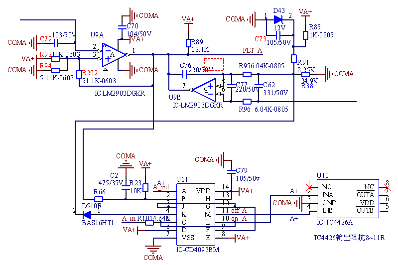
The customer is using CD4093B. On his boards, many CD4093B devices are hot serious. And the supply voltage of 

CS4093B is  pulled low. The customer's schematic is in the attach. VA+ is 15V.

Q1: Can D pin, H pin and E pin be connected to VA+ directly?

Need to add the current limiting resistor in these pins? If they are needed, what is the current limiting resistor value?

What is the current range for the input pin?

Q2: The customer needs to use the output signal of J pin as the input signal for G pin and F pin. 

He also needs to use  the output signal of L pin as the input signal for C pin, like his schematic. Is this OK?

Would you check if the customer's schematic is correct?

Q3: What is the input voltage range? From VN to VDD?

Would you explain what are the VP and VN?

Best Wishes,
Mickey Zhang
Asia Customer Support Center
Texas Instruments

  • Hi Mickey,

    To answer each quesiton directly:

    Q1: Can D pin, H pin and E pin be connected to VA+ directly?

    Yes, as long as VA+ is not larger than VDD (which it cannot be based on the above schematic).

    Need to add the current limiting resistor in these pins? If they are needed, what is the current limiting resistor value?

    No - unless the input is being driven above VDD or below VSS.

    What is the current range for the input pin?

    The input pin usually will have <1 uA of leakage current.

    If the input is driven above Vcc or below Vss, the input diodes will be activated and current will increase. It should be limited in this case to 10mA.

    Q2: The customer needs to use the output signal of J pin as the input signal for G pin and F pin.

    He also needs to use  the output signal of L pin as the input signal for C pin, like his schematic. Is this OK?

    Yes, any output can be connected to the input of any channel.

    Would you check if the customer's schematic is correct?

    What is the signal at A_in1?

    Overall, it looks fine. A slow input that stays near the thresholds for long periods could cause some shoot through current, but I would be surprised if it caused overheating. Can you get a reading of the supply current into the device during operation?

    Q3: What is the input voltage range? From VN to VDD?

    The input voltage range is identified on page 1 of the datasheet as -0.5V to VDD + 0.5V

    Would you explain what are the VP and VN?

    VP is the positive-going input voltage threshold, and VN is the negative-going input voltage threshold. This is a Schmitt-trigger input device, so it has specs for VP, VN, and VH (hysteresis on the inputs)