We want to use TI SN74AVC16T245DGVR to translate DAC CLK and DATA[13:0] from 1.8V (FPGA I/O) to 3.3V (DAC I/O).
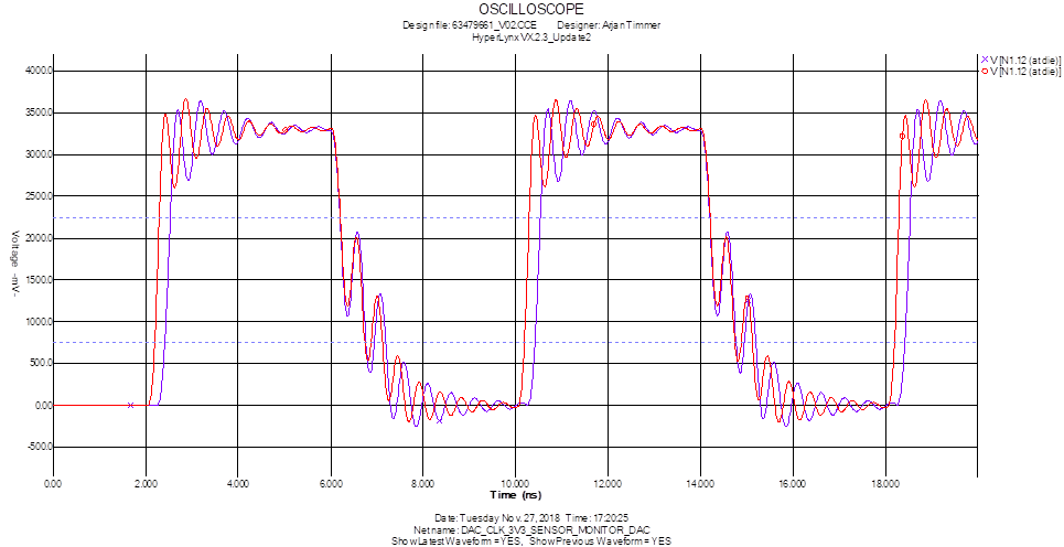
DAC_CLK = 125MHz (tCLK = 8ns).
Schematics:

Layout:

3V3 DAC CLK and DATA[13:0] traces are all on PCB bottom, and routed with 50 Ohm impedance.
Trace lengths are matched and only ~7.0mm long.
SI-analysis was performed on all signals using HyperLynx.
TI SN74AVC16T245DGVR IBIS file is downloaded from http://www.ti.com/lit/mo/scem451/scem451.ibs
Analog Devices AD9707 IBIS file is downloaded from https://www.analog.com/media/en/simulation-models/ibis-models/ad9707.ibs
1.8V signals are fine.
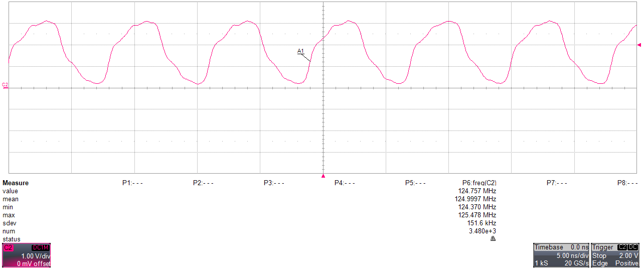
3.3V signals from level-shifter to DAC all look very bad:

The 100 Ohm series resistor that is mentioned as a possible solution is not an option, since there is not enough space on this fully populated PCB.
Besides, risetime and fall time of the signals are very asymmetrical. This makes it more difficult to get proper setup and hold times at the DAC device.
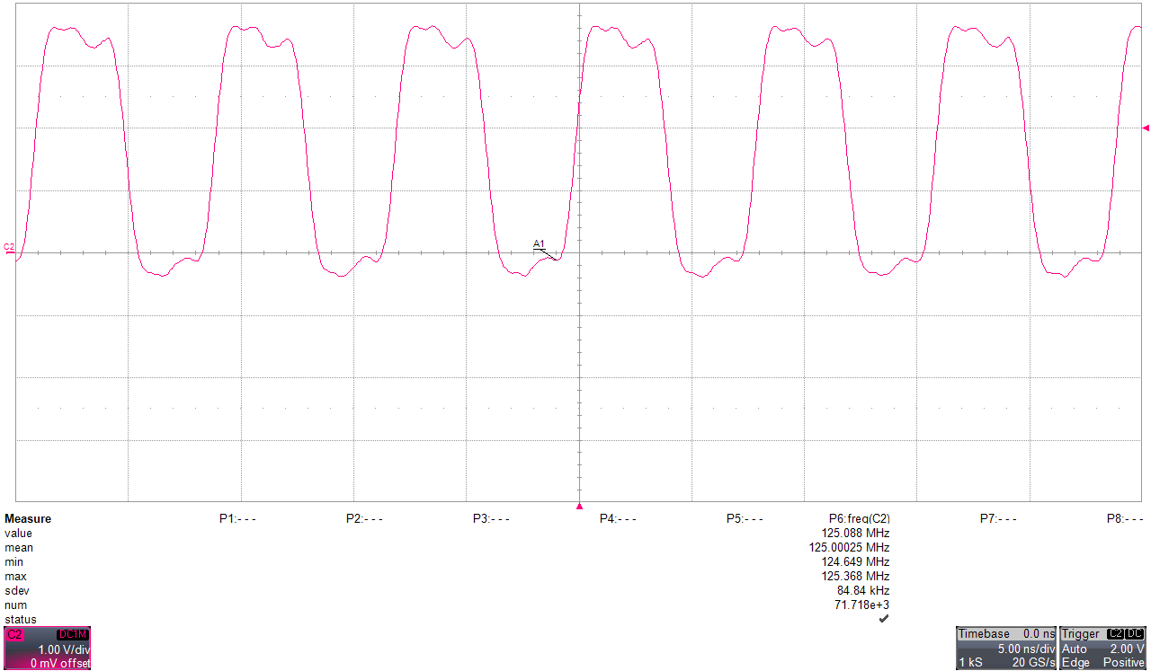
As an alternative a compatible level-shifter from NXP/Nexperia was used in the SI-analysis (74AVC16T245DGV).
https://assets.nexperia.com/documents/ibis-model/avc16t245.ibs
Those results looked very fine, with no excessive ringing and symmetrical edges.
from TI IBIS file: t_fall = ~3*t_rise
[Ramp]
| AVC16T245_IO_33
| variable typ min max
dV/dt_r 1.97/2.35E-10 1.79/3.59E-10 2.16/1.73E-10
dV/dt_f 1.95/7.46E-10 1.78/1.00E-09 2.14/3.31E-10
from NXP IBIS file: t_fall = ~t_rise
[Ramp]
| AVC16T245_BION_33
| variable typ min max
dV/dt_r 1.8726E+00/4.0904E-10 1.6970E+00/5.1595E-10 2.0455E+00/3.8291E-10
dV/dt_f 1.8731E+00/4.1216E-10 1.6981E+00/4.1634E-10 2.0457E+00/4.2922E-10
Can you explain what goes wrong with the TI part?
Regards,
Paul