FAQ: Logic and Voltage Translation > Input Parameters >> Current FAQ
What is VIH and VIL?

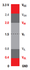
JEDEC - VIH min is the least positive (most negative) value of high-level input voltage for which operation of the logic element within specification limits is to be expected. VIH max is the most positive (least negative) value of high-level input voltage for which operation of the logic element within specification limits is to be expected.
TI - An input voltage within the more positive (the less negative) of the two ranges of values used to represent the binary variables.
JEDEC - VIL min is the least-positive (most negative) value of low-level input voltage for which operation of the logic element within specification limits is to be expected. VIL max is the most positive (least negative) value of low-level input voltage for which operation of the logic element within specification limits is to be expected.
TI - An input voltage within the less positive (more negative) of the two ranges of values used to represent the binary variables.
Here is an example VIH and VIL found in the datasheet for the SN74LVC1G08.
When is the device supposed to switch?
There is a threshold voltage, Vt, that all devices switch at. This threshold voltage is typically slightly less than ½Vcc or ½Vref voltage. For Schmitt-Trigger input devices, there are two thresholds, VT+ and VT- (found in the datasheet) which are not to be confused with the VIH and VIL values. Because the device should switch faster than the input transition rate mentioned in the datasheet, it can be difficult to find the exact value of the threshold voltage.
For a Vcc of 5V for example, the SN74LVC1G08 will switch at around 2.5V. However the input should always be above .7*Vcc to ensure a logic high, or below .3*Vcc to ensure a logic low, except during switching. The transition between the low and high levels should be faster than the input transition rate mentioned in the datasheet table provided, to avoid high Icc current, internal oscillations, and reduction in reliability.
If the device switches at ½Vcc, why do I need to operate above or below VIH and VIL respectively?
Failure to supply a voltage to the input of a CMOS device that meets the VIH or VIL recommended operating conditions can cause:
(1) propagation of incorrect logic states
(2) high ICC currents
(3) high input noise gain and oscillations
(4) power- and ground-rail surge currents and noise
(5) catastrophic device and circuit failure
It is imperative that for any logic device, but especially for a CMOS input, the input always be above or below the recommended VIH min or VIL max, respectively. Failure to do this causes a surge of current to flow through the input inverter from the VCC supply to ground and, subsequently, may destroy the device.

