This thread has been locked.

If you have a related question, please click the "Ask a related question" button in the top right corner. The newly created question will be automatically linked to this question.

SN74LVC14A: SN74LVC14APW: input port protection circuit

Part Number: SN74LVC14A

Hi,

I have some questions regarding the input port protection circuit (if there are any) for the SN74LVC14APW.

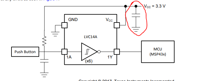
This IC  is applied to the push button debounce circuit.

Phenomenon: IC  input port  of PIN1 is damaged. After the IC is damaged, the following testing is carried out.

                         The resistor value of input pin1 and  pin7(gnd)is low impendence(about 300Ω)。

                         The voltage value of pin1 and pin7 is about 0.3V using the Multimeter's diode gear testing.

Question: 

Q1: Which condition can cause the pin to be damaged. 

IF I want to reappear the damage case, How to operate?

Q2: Can we have the equivalent circuit of  SN74LVC14APW  input port ?

  • Hi,

    It is hard to say what condition will cause the damage on the pin. The device has CMOS inputs. The input should be high impedance.

    There is a clamp diode between GND and Input pins. So there should be one diode drop from GND to the input.

    This thread talks about slow signals on CMOS inputs. However, you are using schmitt-trigger inputs so slow inputs are not a problem for you.

    https://e2e.ti.com/support/logic/f/151/t/737694?tisearch=e2e-sitesearch&keymatch=faq%3Atrue

    Can you provide a schematic for your debounce circuit? And scope shots of input and output signals?

    Thanks!

    -Karan

  • LVC inputs have an ESD protection diode from GND to the pin for negative ESD events, and the equivalent of a Zener from the pin to GND for positive ESD events.


    That ESD protection is designed for what happens during PCB manufacturing using automated machinery; anything that can be touched by humans needs more protection. It sounds as if you have ESD damage.

    Try adding two Schottky diodes in series (e.g., BAT54S) from GND to the pin, and from the pin to VCC.

  • to TI.pptxDear Karan


    Thanks for your answer。

    The releated schematic is attached.

    During Practical application, Vin is Priority over Vcc.

  • Hi Gura,

    Thanks for your reply.

    Could you provide the internal equivalent logic circuit Diagram?

  • Hi,

    It is hard to tell if anything is wrong with your limited schematic. Do you have decoupling caps on your device supply? How often is this damage occurring?

    What is the resistor value from your 5V source? 

    This is a video on the circuit for a debounce switch.

    This is an equivalent input diagram.

    Thanks!

    -Karan

  • Dear  Karan,

    Thaks for your reply。

    >>What is the resistor value from your 5V source? 

    >>Do you have decoupling caps on your device supply?

    Answer is as belows.

    The pulled up resistor's value is 1K。

    The decoupling caps's value is 470pF.

    I want to ask a question about the  decoupling caps.

    For the switch input port, generally, how much value to select of  Decoupling Capacitor ?

    Could you give me some advice?

    Thanks!

    Sincerely

  • Hi,

    By a decoupling capacitor, I mean a capacitor that goes from Vcc to GND, very close to your IC.

    A 0.1-µF bypass capacitor is typically recommended. You can look at the power supply recommendation section of the datasheet.

    Secondly, please watch the debounce video that I provided in my last response. I believe your 1kOhm and 470 pF RC combination will not be enough to debounce your switch. I would recommend using a 10kOhm and 1uF capacitor to do it.

    Thanks!

    -Karan

  • Dear Karan,

    As you said in our circuit, the bypass capacitor is actually 0.1uf。

    Thanks for your advice of RC combination.

    But on the MCU side, there is a software debounce processing. So I think it would be enough to debounce the switch.

    Now,my question is that the input port(Vi)is damaged that has  happend.

    The voltage of  the input port is about 0.3V  and low impedance.

    What reason can cause this damage?

    which part is invalid of the device as you shown the equivalent input diagram?

    Is clamp diode damaged or the other parts?

    Which kinds of voltage(Positive Voltage or Negative Voltage) is more likely to damage the device(Such as internal clamp diode ect..)?

    Please give me your assistance and answer the questions above.

    Thanks!

    Sincerely.

  • Hi,

    What reason can cause this damage?

    Since the button is a manual switch that someone has contact with, you need to have ESD protection.

    The damage is most likely due to ESD.

    which part is invalid of the device as you shown the equivalent input diagram?

    Is clamp diode damaged or the other parts?

    ESD damage can be very random. It is hard to tell without opening up the part what has been damaged.

    Since you said the inputs are shorted to GND, it is very likely that the input clamp diode has been shorted. But hard to say for sure.

    Which kinds of voltage(Positive Voltage or Negative Voltage) is more likely to damage the device(Such as internal clamp diode ect..)?

    Any ESD voltage that pushes the device outside the datasheet specs can cause damage. It is nearly impossible to predict impact of ESD damage.

    Thanks!

    -Karan

  • Dear Karan,

    Thanks for your several replies.

    But I still have some questions to consult you.


    I have opend up the failure part, the attached file is the inspection result with microscope and X-ray.

    Could you take a look at the inspection result?

    and give us some your assertion if wherther this observation can provide the evidence of exact ESD reason.

    If I want to find the most exactly reason,I should to do which test about the failure IC?

    Please give your advice.


    The other question is the sequence of the IC application.

    For this IC chip,the voltage of Vin(5V)supplied is prior to the Vcc(3.3V)supplied.

    Generally is such application  allowed in this case? is there any effect on the chip?


    Look forward to hearing from you.

    Thanks!

    inspection result.pptx


  • Hi,

    I can't analyze from just looking at the images. I would recommend you start an FA with your distributor to find the cause.

    As I mentioned before, there are multiple ways the device can be damaged. If there is a negative voltage that drives too much current through the ESD diode, it can be damaged. If there is higher than recommend input voltage, you can damage the CMOS inputs. If its ESD, either of those things can happen. So it will be hard to tell for sure what caused the damage even after looking at it.

    I will reiterate that the ESD protection provided on the part is only for protection during manufacturing and not for when the device is in use. It is highly recommended to add external ESD protection when there is user input like a switch.

    The device doesn't have a positive clamp on the input so the input of the device can be greater than Vcc without any damage. It is okay to have 5V at the input when Vcc is at GND or 3.3V. Will not cause damage to the part.

    Thanks!

    -Karan