This thread has been locked.

If you have a related question, please click the "Ask a related question" button in the top right corner. The newly created question will be automatically linked to this question.

SN74LV165A: SN74LV165A Outputs not changing state

Part Number: SN74LV165A

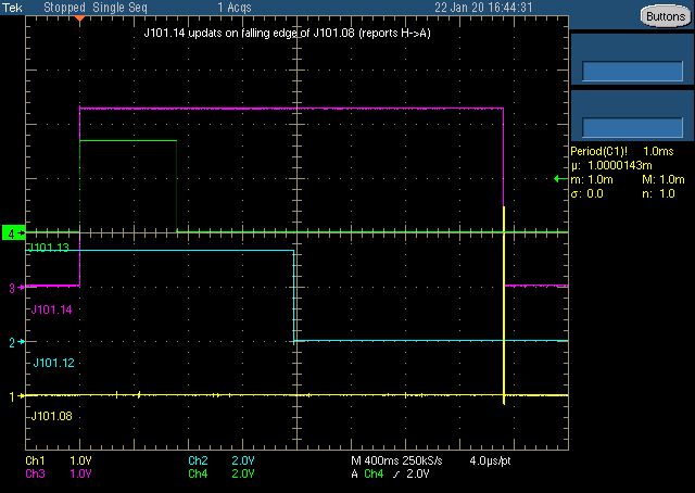
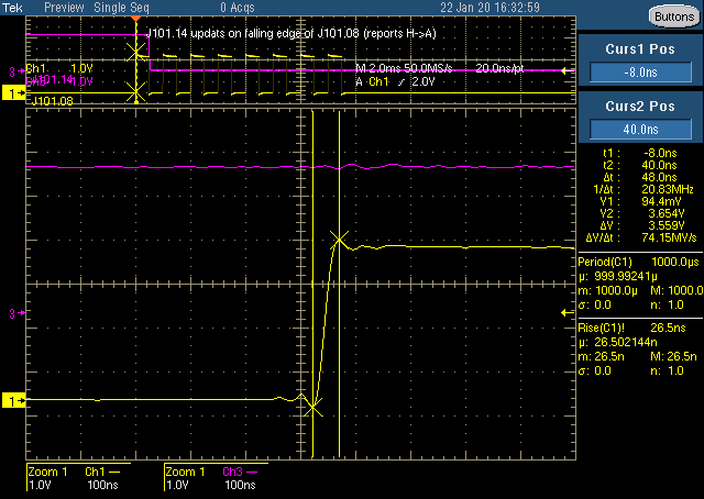
I'm using the SN74LV165A in one of my prototype designs and cannot get the Q_H or \Q_H output to change states.  The Q_H remains LOW while the \Q_H remains HIGH.  Two of my parallel inputs are set HIGH with the rest LOW for this scenario, and SER is pulled LOW as well.  I've sent the \LD pin LOW for ~1sec then send my 8 clock pulses (1ms 50% duty cycle) to the CLK pin (while CLK_INH set Low).  But the outputs do not change states and instead remain static.  I've tried this on 3 devices so far with the same results.  The only thing I can think of is that the Low SER input is somehow overriding the parrallel H-A inputs, but I dont see anything in the datasheet related to such a thing (other than the first page wherein \LD held Low is independent of CLK, CLK_INH, & SER states).

The first time after power-up that I send the \LD pulse, the Q_H goes from Low to High.  Then when the CLK pulses are sent, the Q_H goes from High to Low and stays there.  I have tried various clock pulse widths with no impact to output.

Any insight on why the outputs would not be changing would be greatly appreciated.

  • Hi Jeff,

    Can you please provide scope shots of your inputs? Can you also provide a schematic, specifically what is connected to your outputs?

    I would like to know what voltages and frequencies you are operating at.

    Thanks!

    -Karan

  • Schematic attached below.  J101 is a connector, and J101.14 (output) is only loaded by the scope probe.  J101.12 is now acting as my Clock Inhibit signal wherein I apply 3.3V to the connector pin to inhibit, and J101.08 I apply 0 to 3.3V clock pulses.  The clock inputs are being used in this manner to better align with the datasheet recommendation (i.e. CLK is default High so that when Inhibit is asserted/de-asserted there is no incidental shifting).  Thus, I expect my J101.14 pin to "update" or shift on the falling edges of the J101.08 pin.  The scope shot below is after sending a ~1sec high pulse to J101.13 (providing a low pulse to \LD).  Input measurements for H-A on the schematic are from a DMM during the \LD pulse (levels are steady for a few seconds prior to sending the \LD pulse).

    Thanks,

    Jeff

  • Hi Jeff,

    Can you please zoom into your clock signals so I can see what your rise and fall times of that clock signal is? You need a faster than 100ns/V rise and fall time.

    When you say you set the clock inhibit high, I am assuming that  inverter sets it low afterwards?

    Can you also include a scope shot of you Loading the device with the load pin?

    Thanks!

    -Karan

  • Attached are scope shots of the timing inputs and the sequence I perform them.  Also included is a zoom in of the clock signal rising edge.  Doesn't the SN74LV165A datasheet call for input dt/dV rates ≤ 100ns/V?  I also tried injecting a sine-wave for slower rise times instead of a square wave but didn't see any change in the output.  I'm using connector pin 12 as my clock inhibit (chip pin 2) so that the pin being clocked (chip pin 15) will default high due to the inverter and prevent inadvertent shifting as the inhibit toggles between Low and High as needed.

    Thanks again,

    Jeff

  • Hi,

    Your transition rate needs to be fast. Do not put sine waves at your inputs, it will damage the devices. Can you show me zoomed in scope shot of the negative edge of your clock when the output shifts low? Can you also provide the zoomed signal of the transitions at the pin out of shift register at pin 15 (I want to know  the output of the inverter, not what you are inputting) There may be something wrong with the inverter. Can you also give me a zoomed in shot of the purple waveform (Q) going low? Might be able to see the oscillations there.

    Thanks!

    -Karan