Hi team,
My customer is using SN74LVC1G08 with VCC=3.3V power supply. And the input signal is 0V/5V level. According to our datasheet, SN74LVC1G08 can handle 5V input when VCC=3.3V. So my customer has below question for this use case. Thanks.
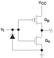
1. Can you help provide the internal structure of SN74LVC1G08 input stage to show how it can handle 5V input when VCC=3.3V? Customer wants to know more detail about the internal structure while our datasheet doesn't have it.
2. Is there a internal clamping diode between input pin and the VCC power supply to protect the device under the use case of input=5V and VCC=3.3V ? if so, do we need to add a current limit resistor on the input pin to limit the input current?
3. When VCC=3.3V, is the power consumption of 5V input use case higher than 3.3V input use case?
Best regards,
Wayne


