Other Parts Discussed in Thread: SN74LVC8T245
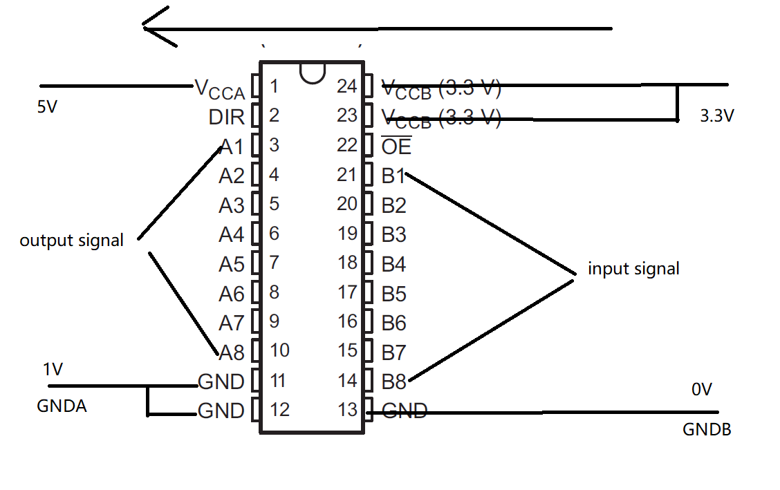
This is a special application of SN74LVC4245A , GNDA is the ground of output signal which is 1V above input signal ground(GNDB). customer perform test and found PIN11&12 and PIN13 are disconnected, so they separate the PORTA GND(PIN11,12) and PORTB GND(PIN13), showed as below chart, now the circuits works well. Still has two question need your help here:
-
Is PIN11&PIN12 independent to P13 inside chip? Is ok to put 1V on PIN12&PIN and 0V on PIN13?
-
If the answer of above question is yes, what is minimum voltage of VCCA,?