This thread has been locked.

If you have a related question, please click the "Ask a related question" button in the top right corner. The newly created question will be automatically linked to this question.

SN74LVC1G123: About 1 in 500 failure on production line

Part Number: SN74LVC1G123
Other Parts Discussed in Thread: SN74LV221A

I have a puzzling case of a not so rare failure of the SN74LVC1G123DCTR part in production.
I am seeing occasional (perhaps 1 in 500) failures of the SN74LVC1G123DCTR to function correctly.
The failure mode is perplexing too, in that it may fail to function at room temperature, but will begin functioning correctly at elevated temperature, or may function correctly at room temperature, but will fail to function correctly at a slightly lower temperature.

I have included my schematic around the SN74LVC1G123DCTR, which I have designed to pulse a MOSFET on for a fixed period in an oscillator flyback voltage boost design.
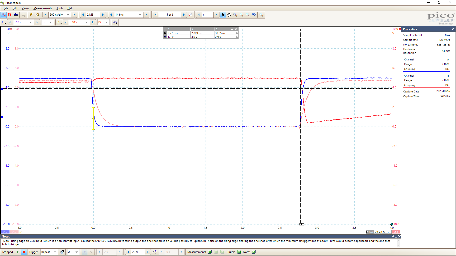
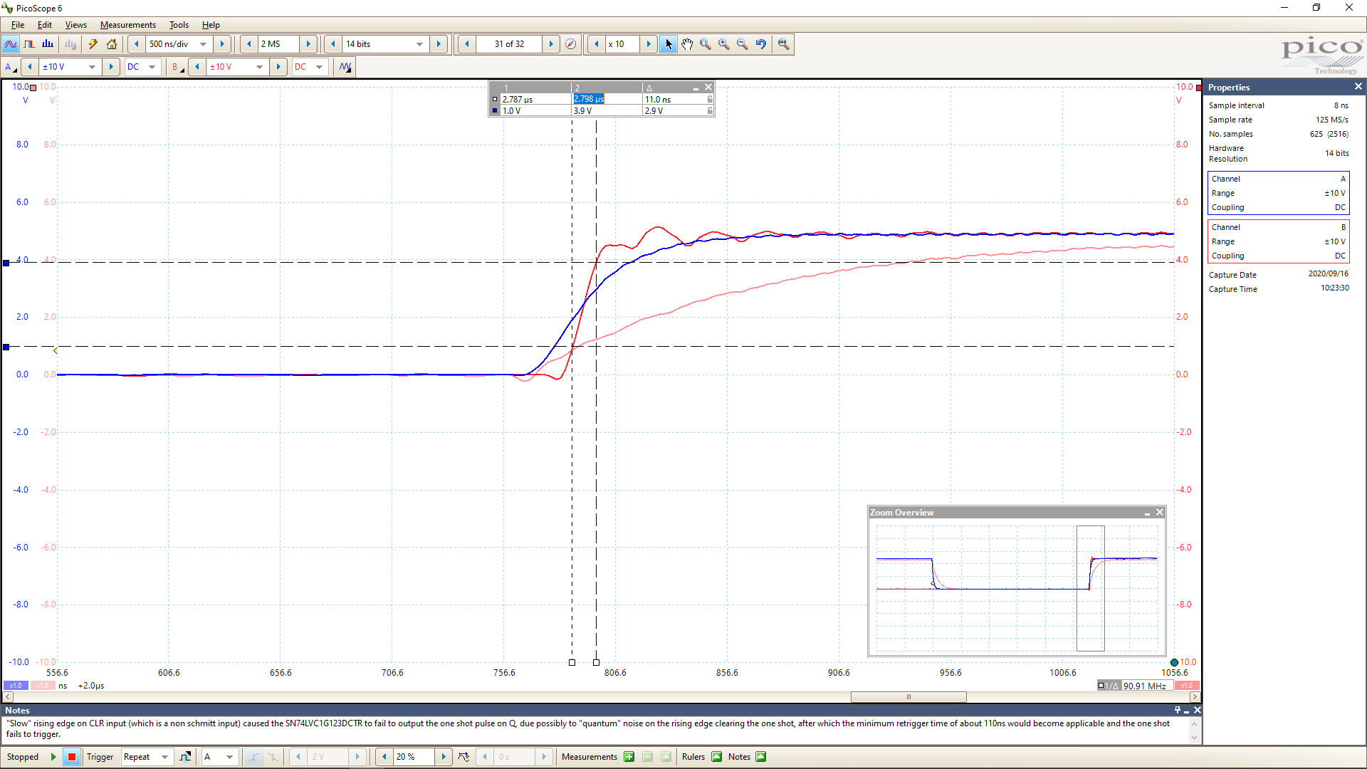
The failure mode is that the output Q, simply does not go to logic high for the one shot period as one would expect under the following condition;
With input A(BAR) bonded to circuit 0V, input B pulled up with 47k and CLR(BAR) initially held low (tied to an MCU IO pin).
When the CLR input is taken high and held high, no one shot pulse appears on the Q output.
The MCU firmware then continues to pulse the CLR input, low for 5uS and high for 2ms on an ongoing basses attempting to start the oscillator (flyback) process.

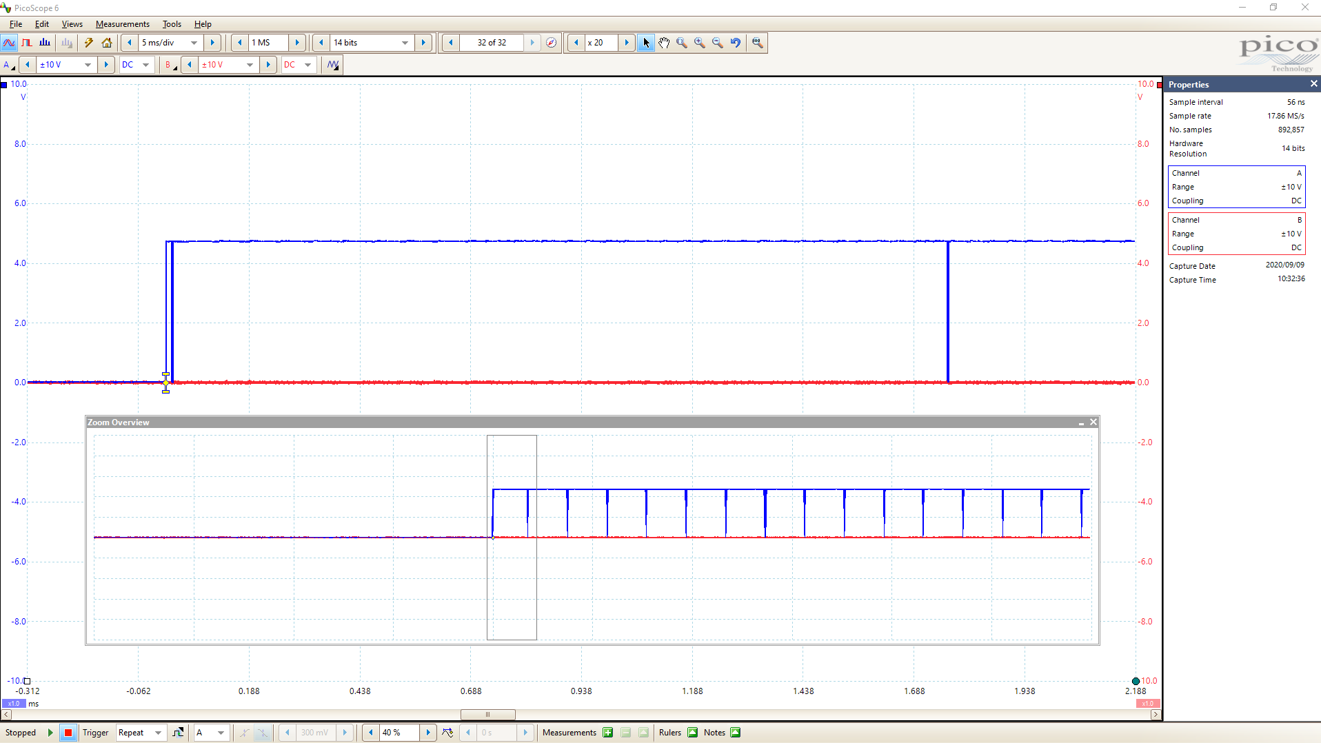
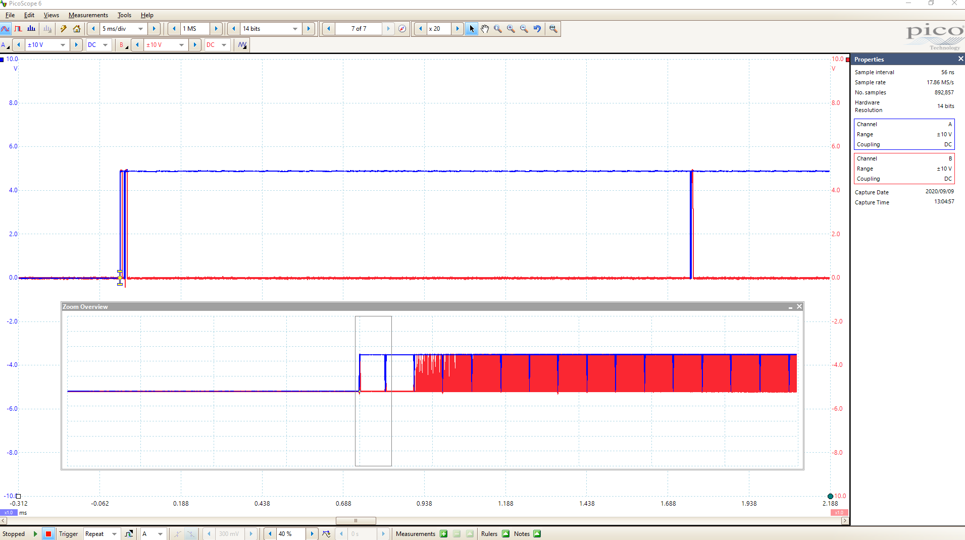
I have included 2x scope screenshots.
Ch-A the blue trace, probe is on the CLR input.
Ch-B the red trace, probe is on the Q output.

The "TI fail to OSC" file shows that the one shot is not raising the Q output to high at room temperature and the "TI osc at temperature" shows the same capture and circuit functioning when heated with a hot air pencil.

I have seen this type of fault once previously in my many decades old career as a development engineer.
The cause back then on that occasion was due to a bond out wire going open circuit when the SMT package cracked during IR soldering due to moisture ingress into the SMT parts in stock.
The SN74LVC1G123DCTR part seems to not indicate any moisture sensitivity in the data sheet or packaging though?

I appreciate any feedback on this issue.

  • Hi Shaun, and welcome to the forums!

    Can we get a view of the CLR\ input & Q output together with a smaller time scale (100ns or less per division, looking at edge rate/signal integrity)?

    Also two more -- one showing a single output pulse when it's  working & another when it's not -- including 3 locations in the circuit - the trigger (CLR\), output (Q), and the RC timing node (Res/Cap). Timescale on this one will have to be larger to capture the pulse width (maybe 200us per div?)

    From the schematic, I don't see any problems besides possibly a slow input transition at the CLR\ pin, but I'd like to see the waveforms to have a better idea of where the issue might be. Also, can you tell me what temperature things fail / work at? An estimation is OK if you aren't using a temp chamber.

  • Thanks for your reply Emrys.

    I was not aware of this e2e.Ti forum until a couple of days ago.

    I found this post with much the same symptom as myself; https://e2e.ti.com/support/logic/f/151/p/920410/3401775
    It would seem that the SN74LVC1G123 is excessively sensitive to the rate of rise of the CLR input to the point that the Q output pulse does not get generated if the rate of rise is too "slow", which in my design with R9 = 4k7 is 120ns (20% to 80%)

    The big question now is;
    Exactly what rise time does the SN74LVC1G123 actually require to guarantee correct operation over the full operating temperature range of the device?
    I would have expected that if this parameter is as critical as it seems to be, that the maximum rise time of the CLR input be documented in the data sheet of the device.

    In my design, reducing R9 from 4k7 down to 1K seems to have corrected the faulty operation, at room temperature, of this one identified device.
    The rise time is now measured at 33ns (20% to 80%).
    R9 is placed in circuit as a current limiting component to save the MCU should something fail in the flyback circuit around the SN74LVC...

    Even if R9 was to be reduced to 0 ohm, the rise rate of the MCU pin is limited to around 15ns (20% to 80%), but of course the question remains for the SN74LVC1G123 CLR input, just how fast is fast enough?

    Regards
    Shaun

  • Hey Shaun,

    I agree that this device should have had an input transition rate specified for the non-Schmitt-trigger input. It also should have had input threshold values specified instead of just VIH and VIL for all Schmitt-trigger inputs.

    Fortunately there are other devices in the same family that we can refer to for those details, but, as you have pointed out, it can cause confusion for system designers.

    For a standard CMOS input, input transition rate should be very fast. Having a slower input transition rate on non-Schmitt-Trigger inputs can cause internal oscillations and functional failure -- not just on this device, but on any CMOS logic device.

    I grabbed the ROC table from another LVC family device which includes the recommended input transition rate for standard LVC-family CMOS inputs:

    This kind of issue doesn't always happen, as you have discovered you might only see it occasionally, but we always recommend keeping those input edges fast for CMOS inputs.

  • A quick response to more directly answer some of your queries;

    The temperature that this particular sample transitions at is, non functional up to about 80 deg C and then functional from 80 deg C and hotter.
    So I assume transistor gain related.
    Another unit I tested, became functional once I applied pressure by pressing on top of the package with a screwdriver, which jogged the memory of my experience with a fractured package breaking a bond out wire. (It is however possible that that particular unit was a red herring and in fact may have been a poor solder joint, even though I would say it is unlikely that that was the case, as the joints had been inspected with a magnifying glass.)


    Ch-A (blue trace) is the CLR input after changing R9 to 1k.
    The light red trace is a reference capture of CLR when R9 was still set at 4k7
    Ch-B (Red trace) is the RC pin and can be seen to be functioning correctly with the faster rise time on CLR, where as previously is stayed permanently high and Q remained permanently low.

  • Thanks Emrys.

    As I am running with a 4.9V VCC supply, according to the above ROC table, my 24Mhz MCU should have IOs capable of 5ns rise time and not the 15ns it does have. Hmmm, those are tough rise rate to achieve and also undesirable from a radiated emissions view point, but these are now my problem ;-)

    "Slow" transitions on CMOS inputs, even the old CD4000 series have always existed, but the end result I have only ever seen is slight higher power consumption, and of course pulse edges that may have "chatter". Never have I seen a complete failure to transition to a final expected state.

    Thanks for your input on this issue, Cheers ;-)

  • I accidentally clicked the "TI thinks resolved" button on this post - sorry about that.

    The image didn't come through for me.

    I think we've found the issue though -- slow inputs can cause problems.  If you want to get a more thorough analysis, you could submit an FA with the failing units through your supplier and we can get detailed physical and electrical tests done of each unit that is give you trouble.

    Usually one of the first steps for an FA would be to ask me about the application, and my response will be that a slow input could cause troubles. You might want to bring that up in your submission if you go that route.

  • Hi Emrys. I actually set this issue to resolved yesterday.

    For now, changing R9 on the pick and place machine from 4k7 (120ns rise time) to 1k (33ns rise time) is the remedy to my 1 out of 500 failure rate I have been experiencing.
    The 5ns rise time may be required in noisy circuits but practically for me, thus far, 33ns seems to be more than adequate.
    Should I still experience further failures in production ahead, I still have wiggle room down to 0 ohm (15ns rise time) if need be, before I have to go and modify the PCB design.

    While I still have your attention, does TI have an equivalent or similar part to the SN74LVC1G123 that does not have such a tight tolerance on the CLR rise time, perhaps in a slower CMOS technology, or even better for my use case, and others too it would seem, would be a schmitt input on CLR.

    I include the image that went missing in my last post for your interest.

    Thanks again for your assistance.

  • Perhaps 3rd time lucky. Pasting an image appears to work while editing , but does not show in the final post.
    I have now saved the screen grab as a file and attached the file to this post

  • One last capture for interest.

    I decided to look at the Q rise time of the SN74LVC1G123 and measured it at 11ns.
    Bear in mind that I do have the Q output loaded with a 180 ohm into the gate of a FET capable of Id of 5Amp

    The red trace is the Q output pin, the blue trace is the CLR input after R9=1k and the light red reference waveform is the CLR input after R9=4k7

  • Hey Shaun,

    The SN74LV221A has Schmitt-trigger inputs on all 3 trigger inputs, so that might be an option for you in future projects. It's a larger device - dual channel, but it maybe be worth using instead to avoid any issues.

  • Ahhh, very nice. Triple schmitt! Just what the doc suggested ;-)
    Hmm, triple the cost and size too...but I'll certainly keep the part in mind.

    Thanks again for your assistance, Emrys, and all the best to you.

    Over & Out, regards
    Shaun

  • Happy to help Shaun.

    Feel free to come back any time - I'm always here :)