This thread has been locked.

If you have a related question, please click the "Ask a related question" button in the top right corner. The newly created question will be automatically linked to this question.

TXS0108E: 2 questions about TXS0108E

Part Number: TXS0108E

Hi team,

My customer is using the TXS0108E now and have several questions want to double check with you.

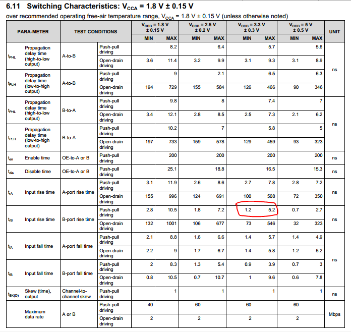
1) We want to check the data with red circuit is test result or input requirement for 60Mhz. The real application is VCCA=1.8V,VCCB=3.3V, data rate 4Mbps and 2Mbps, whether our device have slew rate requirement?

2) When we do the real circuit design for MDC(push-pull) & MDIO(OD). The schematic is below. We find the 1.8V MDIO input waveform(blue) has 2 slew rate during rising period( slow to fast) which is popular for all the boards. We want to check the reason, could you please help?

Thanks.

  • Hi Frank,

    First, please remove the 1k resistors on the unused channels. The device has internal pull-up resistors, so there is no need to terminate the unused channels. Having a 1k resistor tied to ground will produce a voltage divider circuit with the internal pull-up, which will cause added unnecessary power consumption.

    The 1k on the OE pin isn't necessary, but it can be included if they desire.

    I would also recommend to remove the external 10k pull-up resistors on the B1, B2, B3, and B4 ports.

    After that, can you get us a scope shot showing both the input and output of a single channel?

  • Hi Emrys,

    Whether the device have slew rate requirement? Thanks.

  • Slew rate requirements are specified in section 6.3.

    I guess those values in section 6.11 should be labeled "output" instead of "input" because they describe the result of the edge accelerators.

  • Hi Clemens,

    What's the risks if the slew rate is below 10ns/V? Could you please share more details? Thanks.

  • Emrys Maier said:

    Hi Frank,

    First, please remove the 1k resistors on the unused channels. The device has internal pull-up resistors, so there is no need to terminate the unused channels. Having a 1k resistor tied to ground will produce a voltage divider circuit with the internal pull-up, which will cause added unnecessary power consumption.

    The 1k on the OE pin isn't necessary, but it can be included if they desire.

    I would also recommend to remove the external 10k pull-up resistors on the B1, B2, B3, and B4 ports.

    After that, can you get us a scope shot showing both the input and output of a single channel?

    Hi Emrys,

    please kindly check the information below.

    When remove the A5~A8/B5~B8 1kohm, B1-B4 10kohm, A4 pin  1-in, 1-out as the figure 1 and figure 2.

    figure 1

    figure 2

    2.When remove the A5~A8/B5~B8 1kohm, B1-B4 10kohm, and change the R902 to 1kohm, A4 pin  1-in, 1-out as the figure 3 and figure 4. Also test B4 PIN B side input 2--in-3v3

    figure 3

    figure 4

    2--in-3v3

    We can find remove the A5~A8/B5~B8 1kohm, B1-B4 10kohm will not help. if we change the Aside pull up to 1kohm, the slew rate is improved. But it will make the A side low to 550mv, B side low to 200mv.

     we also tried to change A SIDE pull up to 4.7k, B side will be below 150mv, but A side slew rate has issue. 

    Do you have more ideas?

    Thanks.

  • Hey Frank,

    It looks like the performance in this image is excellent:

    Is there a reason that this is unacceptable?

  • If the slew rate is 10 ns/V or better, you get the push/pull driving parameters. If the slew rate is worse, you get the open-drain driving parameters.

  • Hi Emrys,

    As I mentioned in the first post. We want to check the reason of the A side slew rate. You just copy thte B side waveform. 

    BTW: We can find remove the A5~A8/B5~B8 1kohm, B1-B4 10kohm will not help. if we change the Aside pull up to 1kohm, the slew rate is improved. But it will make the A side low to 550mv, B side low to 200mv.

  • Hi Clemens,

    You can find the A side waveform slew rate isn't good enough. When remove the TXS0108, the slew rate is good. Could you please help check the reason? Thanks.

  • The A-side signal is not driven by the TXS, but by the 1.8 V device. As an open-drain signal, the speed of the rising edges is determined by the size of the pull-up resistor.

    The edges are slower with the TXS because of the increased capacitance (the switch itself has some capacitance, but the line is also connected to the circuit at the other side).

  • Hi Clemens,

    Thanks for your reply. Could you please help check the rise time has two slew rate? 

  • Hi Frank,

    The reason there are seemingly two rates in your signal is likely because of how the TXS works. It connects the two sides when at lower voltages, and has them isolated at higher voltages.  As such, the driving device probably can't handle the total load at the lower voltage, so it has a slow rising edge, but when it reaches a high enough voltage to start isolating the two sides then the load decreases and it can increase the voltage quickly.

    If it's an open-drain driver, then the capacitance on the other side must be much larger.

  • Hi Emrys,

    For the two sides, do you mean the A side and B side? Why B side waveform is ok?(if you mean B side cap is too large). Thanks.  

  • Clemens Ladisch said:

    If the slew rate is 10 ns/V or better, you get the push/pull driving parameters. If the slew rate is worse, you get the open-drain driving parameters.

    Hi Clemens,

    Do we have the open-drain slew rate requirement? Thanks.

  • As far as I know, MDIO always is open-drain.

    If your MDIO signal has a speed of at most 2 Mbps, you can use the TXS (without external pull-up resistors).
    If your MDIO signal has a speed of more than 2 Mbps, you have to add strong pull-ups so that you have faster rise times, or you have to use a different translator (the LSF also needs strong pull-ups).