This thread has been locked.

If you have a related question, please click the "Ask a related question" button in the top right corner. The newly created question will be automatically linked to this question.

SN74LV245A: SN74LV245A

Part Number: SN74LV245A

I have a question about SN74LV245A.
Data Sheet SN54LV245A, SN74LV245A SCLS3820-SEPTEMBER 1997-REVISED SEPTEMBER 2014 has the following description.

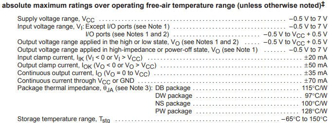
  7.1 Absolute Maximum Ratings

   Vi input voltage range  Except I/O port(2)   MIN -0.5V   MAX 7V
                           i/o ports(2)(3)      MIN -0.5V   MAX 7V

   (2)The input and output negative-voltage rating may be exceeded if the input and output current rating are observed.
   (3)This value is limited 5.5V maximum.


  Question
  ・Is (3) necessary for [I / O port (2) (3)]? Why is it necessary?

   According to Application Report SZZA036C-December 2002-Revised June 2016,
     if there are no clamp diodes between the device inputs and the Vcc supply,
     the positive absolute maximum rating is a limitation of the process technology and is specified as an absolute voltage.

   The TI logic families without clamp diodes in the inputs are ABT, ABTE,--LV, LVC,-- SSTV, and VME.

  • Hello,

    It appears that there was an error during the transcription of this datasheet into TI's new format.  Here's the original table:

    As you can see, the input voltage on the I/O pins should have been limited the same way that the output voltage is, from -0.5V to Vcc + 0.5V.

    This limitation is due to parasitic diodes in the P-channel MOSFETs on the outputs, which share a pin with the inputs.

    It does seem odd that the voltage limitation was chosen to be 5.5V when the process allows up to 7V for Vcc, however, the absolute maximum ratings table isn't intended as a list of functional capabilities, rather a list of worst-case conditions as precursors to damage. Since the device is intended to be operated between 2-V and 5.5-V Vcc, it makes sense for a spec limited by "Vcc + 0.5V" to have this note attached. 

    For example, I would never recommend someone to operate this device with a 6.5V supply and a 7V input voltage. That's a sure recipe for a broken device.


  • Thank you for your reply.

    I understand that Vi is restricted by Vo constraint.

    I also understood that Vi is Max 7V.

    But, I'm sorry.

    Below is a description on Vo of [Absolute Maximum Ratings].

    When Vo is in the [high-impedance] state, Max 7 V.

    When Vo is in the [High or Low] state, Max Vcc + 0.5 V.

    I think the port set for input at the DIR pin will be Max 7 V because Vo is in the [high-impedance] state.

    I think that the port set to output on the DIR pin will be Max Vcc + 0.5 V because Vo is in the [High or Low] state.

    How is this understanding?

  • Hello,
    You are correct. The DIR pin uses the same logic as the OE\ pin, so the effect on the disabled pins will be the same.

    I would still recommend against operating the device at or near 7V.
  • Hello,

    I could confirm that my way of thinking was not wrong.

    Thank you very much.

    In addition, thank you for your advice.

    goodbye.