This thread has been locked.

If you have a related question, please click the "Ask a related question" button in the top right corner. The newly created question will be automatically linked to this question.

CD4093B: Output max current question

Part Number: CD4093B

Hi Team:

Please help to confirm and question as below , thanks.(Datasheet http://www.ti.com/lit/gpn/CD4093B?keyMatch=CD4093B&tisearch=Search-EN-Everything

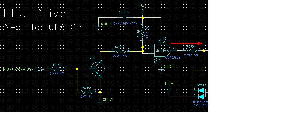
1.When VDD provide 12V and Pin1 & Pin2 with Low and output will high of CD4093B , when output is high level , how is the max current like red arrow as below picture?

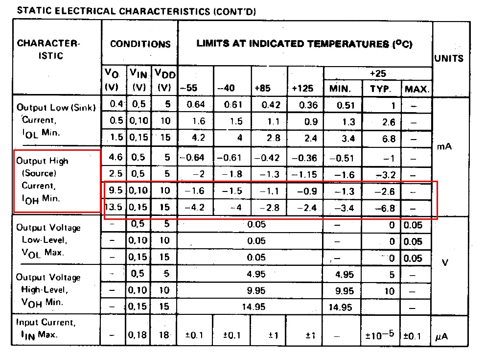
2.Datasheet Only define VDD 10V & 15V on datasheet and define Min & Type , Why not define Max value on datasheet ?

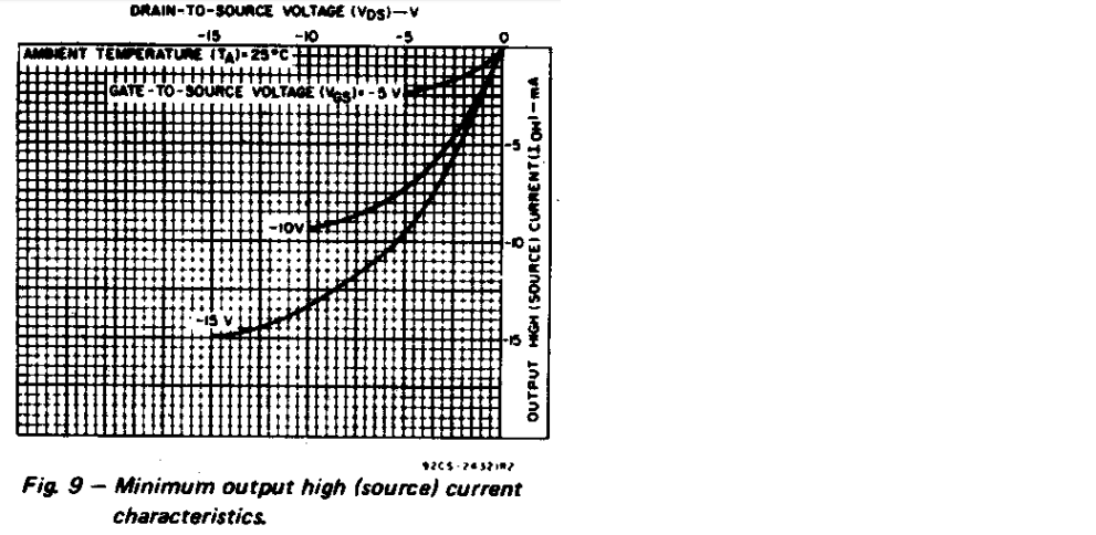
3.Base on Datasheet page 9 and picture as below , What does this curve mean ? What is Vgs and Vds mean ? RD confused could not see any function block about MOSFET ?

Regards / Mark

  • 1. You can interpolate between the 10 V and 12 V values. See [FAQ] What method is best used for estimating specification values between those given in the datasheet?

    2. These values are specified from the point of view of the device, and under the constraint of the test conditions. In other words, at the specified voltage drop (VDD − VO), the chip can provide at least this much current. From your point of view, this is the maximum, i.e., your circuit should draw at most this much current.

    3. VGS is VDD, VDS is VDD − VO. (The output's voltage drop is measured directly at the output transistor.)

  • Hi Clemens Ladisch:

    Please help question as below , thanks a lot.

    1.If VDD=10V,Vo=9.5V, 9.5V/2.6mA=3.65K ohm , it means that output load of resistor can't lower than 3.65K ohm , Am I tight ?

    2.If chosen 1K ohm for utput load of resistor , 9.5V/1k ohm = 9.5mA > 2.6mA(datasheet) , CD4093 can’t provide so much current because of it's define 2.6mA of CD4093 datasheet ?

    Regards / Mark

  • 1. Yes; it means that the ouput load cannot be lower than 3.65 kΩ under the test conditions, i.e., if you want the output voltage to be at least 9.5 V. (And 2.6 mA is the typcial value, not the guaranteed minimum.)

    2. At VDD = 10 V, the typical output impedance is 0.5 V / 2.6 mA ≈ 200 Ω (this is true for currents that are not too large). So you will get a voltage divider of 200 Ω + 1 kΩ, i.e., the output voltage will be approximately 8.3 V.

  • Hi Clemens Ladisch:

    I could not understand question 2 , I mean if chosen 1K ohm for load resistor 9.5V/1k ohm = 9.5mA > 2.6mA(datasheet) , CD4093 can’t provide so much current to 9.5mA  because of it's define 2.6mA of CD4093 datasheet ?

    you mean 10x0.2/(0.2+1K)=1.66 and 10V-1.66V=8.33 V ( IOH_min) =output voltage ?

                     9.5V/2.6mA=3.65K , 10x0.2/(0.2+3.65K)=0.52 and 10V-0.52=9.5V( IOL_min) ?

    Regards / Mark

  • That 2.6 mA is not a limit on what current the chip can provide. It is a limit on what current the chip can provide while the voltage drop over the output transistor is at most 0.5 V. If you try to draw more current, the voltage drop becomes larger, i.e., the output voltage becomes lower.

    This is shown in figure 9 (but for the worst case).


    What is the actual load connected to the output of the CD4093B? A MOSFET gate (which behaves similar to a capacitor)? Are there any pull-down resistors that continuously draw current?