This thread has been locked.

If you have a related question, please click the "Ask a related question" button in the top right corner. The newly created question will be automatically linked to this question.

LSF0204: circuit analysis

Part Number: LSF0204

Hi team,

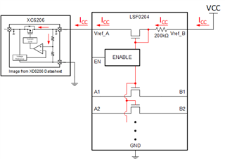
As shown in the schematic diagram, after LSF0204 is welded on, connect 5V power supply and VREF_ The 1.8V at a is raised to 2.7V by lsf0204 chip, which affects the working voltage of other circuits.

Please help to analyze it.

thanks,

Best regards,

  • As shown in the datasheet, the EN and VREF_B pins must be connected together, and need a 200 kΩ resistor to the supply.

    All signals need pull-up resistors; pull-down resistors are not possible.

    The LSF0204 is not suitable for this application. What are the directions of the FSYNC and INT signals?

  • Hi Ladisch,

    Thanks for your reply.

    I add questions.How to change the peripheral of lsf0204 to meet the level conversion between 1.8V and 5V? Lsf0204 specification book clearly written to support 1.8 and 5V conversion ?

    Fsync and int signals are led out from icm20948 for standby, which is not used for the time being.

    Best regards,

  • It's most likely that you have a linear regulator connected to the VREF_A pin of the LSF, which will have to sink some current to provide bias for the device.  Most linear regulators will not function properly if current is sinking into them -- they are designed to provide power by sourcing current.

    If this is the case, you can try adding a resistor from VREF_A to ground to sink this current. A 100kΩ resistor should be sufficient. This can be added directly at the output of your regulator.

  • Hi Maier,

    thank you for your reply.but I don't understand your opinion.

    I want to know how to change the peripheral of lsf0204 to meet the level conversion between 1.8V and 5V? 

    I hope you to explain clearly.

    thank you so much.

  • Hello,

    The first step to operating the LSF0204 is to properly bias the device.  There's a video on this topic located here: Understanding the Bias Circuit for the LSF Family | TI.com Video

    I created the below image to try to explain what I think is going on in your case. I've seen this on multiple occasions.

    As you can see, a current is produced by the bias circuit, labelled above as Icc. This current will flow from Vref_B to Vref_A and then out of the device and into whatever is available to sink the current. In your case, I believe this current is causing your voltage regulator, XC6206, to change the output voltage from 1.8V to 2.7V.

    Can you try to measure this to confirm?

  • Hi Maier,

    Thanks a  lot.

    It is useful.

    Best regards,