This thread has been locked.

If you have a related question, please click the "Ask a related question" button in the top right corner. The newly created question will be automatically linked to this question.

Poor Connectivity - CC2500 PCB Antenna Issue

Other Parts Discussed in Thread: CC2500, CC2510, MSP430F2132

Scenario:

For the past few months I have been working on the communication between two devices with a custom PCB board I have created. Initially I used a chip antenna and encountered a few problems due to incorrect pi-matching and I was unable to resolve that as I did not have the correct equipment.

I have now changed to a PCB antenna and followed the 2510EM PCB antenna reference design very closely (also similar to the AN043 design note) so I can avoid doing this. I am however, using a CC2500 rather than the CC2510 controlled by a MSP430F2132. The location, sizing and components from the RF pins are exactly the same. Please refer to my attachment for the board layouts (1.6 x 43 x 58mm for the receiving board and 0.8 x 30.5 x 50mm for the transmitting board.

On the transmitting board I am sending 5 bytes of data (length, 2xdata, 2xstatus bytes). Both are setup for 250kbaud with CRC checking. This is sending 3 times a second using the MSP430’s timer (going into sleep mode between transmits). On the receiving side I am polling RXBYTES for data. I am however also keeping count of how many packets it actually receives with GDO0 set to 0x06. Please refer to my attached code for further detail in the program side of things, or ask what exactly you want to know so you are able to help.

Problem:

Simply put, the main problem I am getting is bad signal strength, poor transmit distance and high interference if there is objects (hands/bodies) in between the devices. This PCB antenna has been proven to transmit over 200m in LoS (as per AN043), but I am only able to transfer 5-7m before I start to encounter large packet loss. When I have the devices set up 4m apart in clear LoS the receiver receives 99% of the packets being set, and 98% of these pass the CRC check. When I stand in between the devices the amount of packets received will drop to roughly half of what is being sent.

It is also interesting to note that when the boards are in transmit mode, there is the main peak at the selected frequency, however there is noise almost on all channels from the device. Refer to my attachment>TX Mode Spectrum Graphs for the result of two different boards (both the 0.8mm thickness board).

Ideas tested:

  • Tested RX/TX between two 0.8mm board -> thought the board thickness may play a factor, however almost same result between two 0.8mm board
  • Tested in different locations to rule out signal interference, also tested in a 7m Square Hollow Tube. Allowed for slightly longer transmitting distance, but same result when two hands are placed in between the devices.

Still to Test:

  • Different Power levels (Currently at 0dBm on both TX/RX) -> unlikely to work as 0dBm Is already one of the highest gain settings
  • Different frequencies -> unlikely to work as the same problem occurred without signal interference

Help!

Any help with this would be greatly appreciated. I have been at this for months and progress is getting very slow! Ensure why I am getting such poor results with a setup that has been proven before. 

4035.CC2500MSP430 Forum Post.zip

CC2500MSP430 Forum Post.zip
  • I took a quick look at the layout and it looks like you have very poor grounding of the chip? You should follow the reference designs on how to ground the chip.

  • I did follow the reference design and placed the capacitors in the same location in relation to the CC2500 following the layout of the CC2500EM board. I followed the CC2510EM SmartRF for the antenna, and CC2500EM for placement of the surrounding components.

    I would double check the reference designs and anything related to grounding however and let you know if I find any differences. When you refer to grounding the chip, is that mostly related to the surrounding capacitors? 

    Thank you for your reply.

  • The antenna part and the part going from the chip to antenna looks good. But a solid ground plane is required under the chip with as many vias as possible. Also for decoupling caps it is important with a short path from the ground side of the cap back to under the chip. (Ground return path)

  • After looking into it you are very correct, the ground pad under the chip isn't as the datasheet.  I assuming following the design in the CC2500 Datasheet is the safest option?

    Is it common for incorrect grounding to effect transmitting strength/distance?

    I actually got the CC2500 footprint from a 3rd party source... would have liked to think they got it right, note to every to ensure to double check everything you use!

  • For our RF chips you have to have good grounding of the die paddle since this is chip ground.

    For the layout: See http://www.ti.com/litv/zip/swrr016a for how the connection to the chip should be.

    And yes, from experience it will save you time and money to check what you get from a 3rd party, it is surprisingly often it is something wrong somewhere...

  • I am currently redesigning the board.

    Does this look better -> followed the CC2500EM reference design / Datasheet exactly

    I will post how this works when I get the boards here

  • I could not see any layout included in your latest post.

  • Apologies, not sure why it didn't attach.

    Try this: http://i.imgur.com/vP6DNvU.jpg

  • This looks good. Hope you get better performance now.

  • Yes giving the CC2500 a better connection to ground via the correct pad layout made this chip to work perfectly.

    Thank you.

  • Hi

     I have The same problem,  with my  electronic revision  cc2500,

    This electronis system isn't able transfert all packets of the equal distance but the range the transmission is variable with from 3 to7mt.

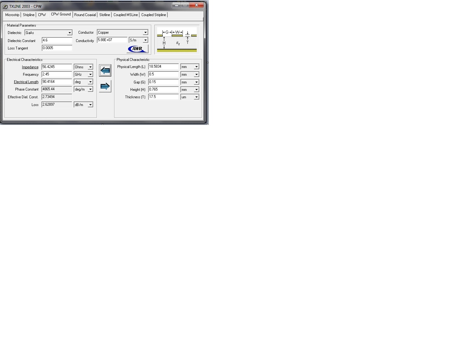
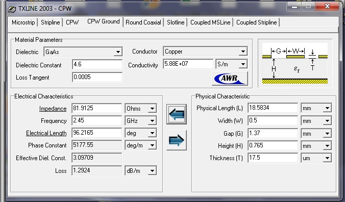
    Old device:I have calcolate a impedance between balun and antenna by Software Txline and it's 81.91 ohm (in attached the picture-Txline old design.jpg)

    I have 3 question for "redesign the trace antenna-balun"

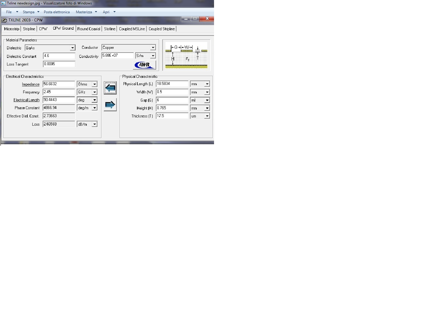
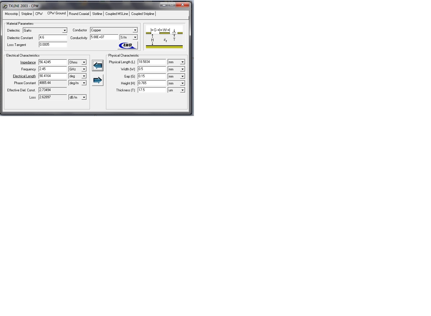
    1)Recalculate and place a new trace between antenna and balun with impedance of 50 ohm, I had calcolate by Txline a impedance of 56 ohm and considering of application a solder mask over antenna  for decrease of 3 ohm(in attached the picture-Txline new design.jpg) 

    2)Recalculate and place a new trace between antenna and balun as described to the point 1 and place a resistor 0 ohm between antenna and trace balun?

    3)The resistor value is 0 Ohm?

    Thank you

    Best Regards

    2627.redesign antenna-balun.rar


  • If you do the calculations a impedance equal to 80 ohm vs 50 ohm does not cause a significant signal loss. Have you checked if it's other details with your design that could explain low range?

  •  The system embedded that in review is realized with radio cc2500 in package smd and also in bonding and in both 2 case the result was the same.

    -low transmission power(distance 7 mt RSSI on average from -72 to -85 DBI with LQI 54)

    -low action range

    The first problem I encountered is that the change of the crystal unit load captance change of value from 13pf to 11 pf  (the crystal unit is 26.0 MHZ SMD 9ppm) this change has improved the synchronization with the transmitter.I did this change considering the high parasitic effects of circuit and pcb.

    Best Regards