This thread has been locked.

If you have a related question, please click the "Ask a related question" button in the top right corner. The newly created question will be automatically linked to this question.

TM4C1290NCPDT: SSI 26bit CLK

Part Number: TM4C1290NCPDT

Hello.

I made SSI-sensor-2ch-IF BOARD with TM4C1290NCPDT.
Currently debugging.
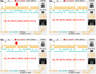
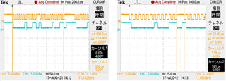
In order to read the data from 25bit-SSI-sensor, CLK13bit was output twice by the SSI module.
However, as Charles worried, there is a delay of 16us or more between 13bit CLKs and it is not possible to read correct data continuously.
Is there a way to read the data by continuously issuing 26-bit CLK?
CLK may be 32 bits.
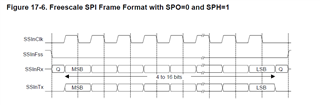
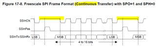
Waveform CH1: CLK, CH2: sensor DATA
The current coding is as follows.
--------
sysclk = MAP_SysCtlClockFreqSet((SYSCTL_XTAL_20MHZ
|(SYSCTL_OSC_MAIN)|(SYSCTL_USE_PLL)) ,20000000);

MAP_SSIAdvModeSet(SSI1_BASE, SSI_ADV_MODE_LEGACY);

MAP_SSIConfigSetExpClk(SSI1_BASE, sysclk, SSI_FRF_MOTO_MODE_0,
SSI_MODE_MASTER, 90000, 13);
while(!SysCtlPeripheralReady(SYSCTL_PERIPH_SSI1));

MAP_SSIEnable(SSI1_BASE);
while(MAP_SSIDataGetNonBlocking(SSI1_BASE, &d[0])) ;
for(i=0;i<2;i++)
{
MAP_SSIDataPut(SSI1_BASE, 0); //out 13CLKS
MAP_SSIDataGet(SSI1_BASE, &d[i]);
}
--------

INO

  • Hi,

      I have some doubt with your code vs. the waveform. In your waveform, the CLK looks like you are in SPO=1 and SPH=0. But in your code you have SSI_FRF_MOTO_MODE_0 which has SPO=0 and SPH=0. Are you having an inversion on your board?

      I have some suggestions:

      - Not sure why you want to have an inversion on the board. If you have an inversion on the board then can you remove it? Once you remove it, can you use SSI_FRF_MOTO_MODE_1 instead. Does the result make a difference?

      - Your sensor has a very odd length for the SSI module to support. Between frames, the SSI module will have a period of inactivity. This is inherent by design. If your sensor cannot tolerate this inactivity then you will need to go with a different solution. 

      - I will suggest you try the bit-bang method. 

        1. Create a timer that generates an periodic interrupt that matches the SPICLK frequency.

        2. In the interrupt ISR, toggle a GPIO pin that simulates the SPICLK

        3. In the interrupt ISR, read the SOMI (RX) data pin from the sensor and left shift by one bit.

        4. Repeat step 1 for 2x26=52 times to simulate the 26 SPICLK required by your sensor. 

      I think the bit-bang method should not be difficult to implement. 

  • Charles
    I'm sorry to confuse you.
    The CLK waveform is not the waveform at the device terminal.
    This is the waveform at the sensor input that is electrically inverted.
    I changed various parameters.
    However, the period of inactivity could not be smaller than 22us.
    Let's try the bit bang method.
    thank you.
    INO

  • With the waveform at the terminal of the device.
    It was found that there was no period of inactivity in PH1.
    However, the 2nd CLK edge is the data change point.
    I want to capture the data at the 1st CLK edge.
    If it is PH0, there will be an inactive period.
    difficult.

    INO