Other Parts Discussed in Thread: SEGGER
I am a digital chip designer and we are embedding an MCU into our next chip.
The MCU core (embedded into the chip) has a 5-wire JTAG port for debug purposes.
We don’t really have 4 or 5 pins on the chip we can use for JTAG … so we would like to explore the cJTAG option instead.
I understand that that XDS110 supports both 5-wire JTAG and the 2-wire cJTAG protocols.
I have done some research on the cJTAG protocol and I am left with two conflicting impressions:
- It is very simple to convert an incoming 2-wire cJTAG protocol to the 5-wire protocol used by the MCU
- There’s a lot to the cJTAG and a 2-wire to 5-wire conversion is more complicated than one might imagine.
I believe that the JTAG 1149.7 protocol was designed to coexist with existing 1149.1 standard, and therefore
a 1149.7 compliant TAP controller may well need to have extra complexity to deal with handling the two protocols.
This leads me to think that the XDS110 may need to provide the necessary hand-shaking so that a 1149.7 TAP
controller can switch from JTAG to cJTAG.
I'm hoping to keep the 2-wire to 5-wire conversion as simple as possible,
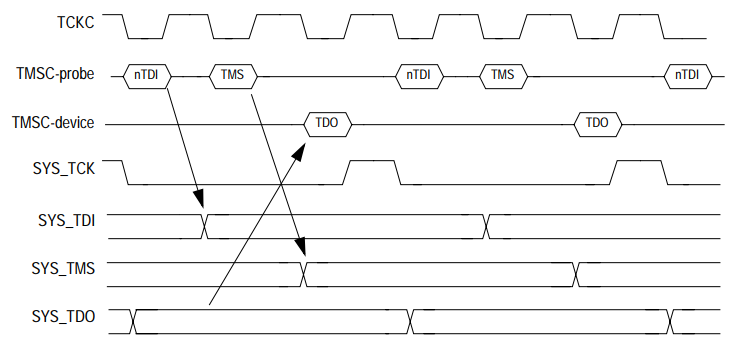
so I'm wondering if I can simply assume an Oscan-1 format as shown below where:
- I assume a triplet (scan-packet) is incoming to the chip from the XDS110
- During the first 2 TCKC low intervals of the triplet I sample TMSC (for nTDI and TMS)
- And during the 3rd TCKC low interval of the triplet I output TDO
- And I forward on the 3rd TCKC pulse to the MCU.
Can I get away with this simplistic approach?
And if so, what timing can I expect on TMSC w.r.t. TCKC (output from XDS110)
and what timing must be met when TMSC is returned to the XDS110.
Any assistance you can offer would be most appreciated.
Thank you.
Andrew