This thread has been locked.

If you have a related question, please click the "Ask a related question" button in the top right corner. The newly created question will be automatically linked to this question.

AM2432: GPMC

Part Number: AM2432
Other Parts Discussed in Thread: SYSCONFIG

Hi Team,

My customer has a question as below.

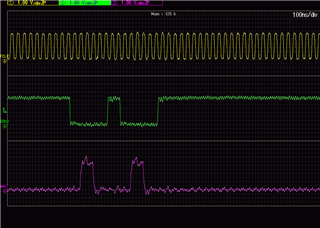
We are doing a 16-bit single read access to the FPGA with GPMC, and we observed a waveform that looks like two accesses are being made. Looking at the address, it appears that the second read is an extra read for the next address.
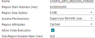
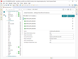
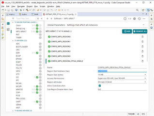
The GPMC setting is Multiplexed address data 16bit device. Please refer to the excel sheet below for the settings/configurations.
Does this phenomenon correspond to errata i2313? 

GPMC Settings.xlsx

If this errata corresponds to i2313, is it correct to say that the errata will be resolved in Rev2, but only one 16-bit access will be made?
Also, according to the errata, it is stated that incorrect data is read when 16-bit read access is performed, but specifically what kind of incorrect data is read? (Does it return the second access data? Returns a random value?)

Best regards,

Mari Tsunoda

  • Hi Mari,

    What are their MPU settings for the GPMC memory address space (0x50000000) in example.syscfg?

    Best regards,

    Ming

  • Hi Ming, 

    I'm attaching the sysconfig file, but they're not sure specifically what settings to show. Since the sysconfig doesn't have any settings for GPMC, could you be more specific if the file linked does not provide you with the right information?

    K9704JF_PERI_0719.syscfg

    Best regards,
    Mari

  • Hi Mari,

    There is no MPU settings at all in your *.syscfg. In order to make the GPMC memory working efficiently, the following MPU region has to be added to your *.syscfg:


    Please refer to the example.syscfg in the MCU+ SDK examples for the common MPU regions

    Best regards,

    Ming 

  • Hi Ming,

    Here is an image of what they see on SysConfig. Where can they change the GPMC settings like you have indicated? 

    Best regards,

    Mari

  • Hi Ming,

    Nevermind, I see what you mean. 

    Thanks for the support. I will let them know.

    Best regards,

    Mari Tsunoda

  • Hi Mari,

    Add a new CONFIG_MPU_REGION6 in MPU ARMv7:

    Best regards,

    Ming

  • Hi Ming,

    The issue still persists even after setting the MPU regions. Do you think this is related to the errata i2313? 

    Also, with regards to setting the MPU regions, how should they decide what regions to set? They followed the example, but are not sure if they have to set it for every memory and peripheral. 

    Best regards,

    Mari

  • Hi Mari,

    Can they use the 32 bit read instead? At least, to prove it is related to errata i2313.

    Best regards,

    Ming 

  • Hi Mari,

    Can they also share their modified *.syscfg file?

    Best regards,

    Ming

  • Hi Ming,

    I will ask them tomorrow during the meeting. Is there anything else I should ask for other than the new sycfg file and using the 32-bit read?

    Best regards,

    Mari

  • Hi Mari,

    No. Those two items are all we need at this point.

    Best regards,

    Ming

  • Hi Ming,

    Ok great! 

    Also, with regards to setting the MPU regions, how should they decide what regions to set? They followed the example, but are not sure if they have to set it for every memory and peripheral. 

    With regards to the MPU regions, is their understanding correct? I'd like to give them some feedback during the meeting.

    Best regards,

    Mari

  • Hi Mari,

    The ARM MPU region was set up in order. The later regions overwrite the previous ones. For example, the CONFG_MPU_REGION0 is the default one which covers 2GB starting address 0x0. It was set to "Supervisor RD+WR, User RD" and "Strongly Ordered". It is good for all the MMR for peripherals.

    The CONFG_MPU_REGION1 is for TCMA 32KB starting at address 0x0. Since the region1 is overwritten the region0, so the 32KB starting address 0x0 becomes  "Supervisor RD+WR, User RD", "Cached" and "Allow Code Execution", the rest of the 2GB remains the same as defined in region0.

    The CONFG_MPU_REGION2 is for TCMB 32KB starting at address 0x41010000. Since the region2 is overwritten the region0 and region1, so the 32KB starting address 0x41010000 becomes  "Supervisor RD+WR, User RD", "Cached" and "Allow Code Execution", the rest of the 2GB remains the same as defined in region0.

    The CONFG_MPU_REGION3 is for OCRAM 2MB starting at address 0x70000000. Since the region3 is overwritten the region0, region1 and region2, so the 2MB starting address 0x70000000 becomes  "Supervisor RD+WR, User RD", "Cached" and "Allow Code Execution", the rest of the 2GB remains the same as defined in region0.

    The CONFG_MPU_REGION5 is for DDR 2GB starting at address 0x80000000. Since the region5 is overwritten the region0, region1, region2  and region3, so the 2GB starting address 0x80000000 becomes  "Supervisor RD+WR, User RD+WR", "Cached" and "Allow Code Execution", the rest of the 2GB remains the same as defined in region0.

    What they need to add is The CONFG_MPU_REGION6 is for GPMC 8MB starting at address 0x50000000. Since the region6 is overwritten the region0, region1, region2, region3 and region5, so the 8MB starting address 0x50000000 becomes  "Supervisor RD+WR, User RD+WR", "Cached" and "Allow Code Execution", the rest of the 2GB remains the same as defined in region0

    Best regards,

    Ming

  • What they need to add is The CONFG_MPU_REGION6 is for GPMC 8MB starting at address 0x50000000. Since the region6 is overwritten the region0, region1, region2, region3 and region5, so the 8MB starting address 0x50000000 becomes  "Supervisor RD+WR, User RD+WR", "Cached" and "Allow Code Execution", the rest of the 2GB remains the same as defined in region0

    Given the described issue was an unwanted extra read seen by a FPGA connected to the GPMC, should CONFG_MPU_REGION6 be set to "Strongly Ordered" rather than "Cached"?

    If the region is marked as "Cached" the CPU could potentially generate speculative reads which could generate extra reads to the FPGA over and above those in the program.

  • Hi Chester,

    Thank you so much for your correction, yes, it should have been the "Strongly Ordered" instead of "Cached"

    Best regards,

    Ming

  • Hi Chester, Ming,

    Thanks for the input. I asked them to send results for the 32-bit read as well, and will follow-up with some additional information including the new syscfg file later. If they are reading from a 16-bit device, wouldn't the 32-bit read result in a similar waveform as the 16-bit read issue they are seeing here? If so, they cannot use the 32-bit read with their 16-bit deviced.

    Best regards,

    Mari

  • Hi Mari,

    With the proper MPU settings, they should not see the two accesses case anymore.

    Best regards,

    Ming

  • Hi Ming,

    Thanks for your reply. Unfortunately it seems that they are still seeing two accesses. I am attaching the syscfg file. Is there any other possible causes for this such as the errata mentioned in the beginning?

    K9704JF_PERI_0719_mcur_r1.syscfg

    Best regards,

    Mari Tsunoda

  • Hi Mari,

    The starting address for Region6 missing one '0'. It should have been 0x50000000.

    Best regards,

    Ming

  • Hi Ming,

    Thanks, will ask them to fix.

    Best,

    Mari

  • Hi Ming,

    Even after they fixed the address, they saw the same result. I have attached the waveform as below. Any other possible issues? Is this related to the errata mentioned in the original thread?

    Best,

    Mari

  • Hi Mari,

    I talked to our AVV team. Here is what they came back:

    -----

    I looked at the waves, the phantom cycles are due to the masked byte enables in the requests made to GPMC, and translation from a 64-bit CBA bus to 32-bit OCP bus.

    For example, in the waves, one of the a CBA write to GPMC is

                    Addr = 0x1000_0000, bytecnt = 0x10

    byten = 0xF0, data = 0x0000_0001_0000_0000 (1st data phase on 64-bit CBA bus)

                    byten = 0x0F, data = 0x0000_0000_0000_0002  (2nd data phase on 64-bit CBA bus)

    This translates to OCP write

                    Addr = 0x1000_0000, burst_len = 0x4

    byten = 0x0, data = 0x0000_0000 (1st data phase on 32-bit OCP bus)

    byten = 0xF, data = 0x0000_0001 (2nd data phase on 32-bit OCP bus)

    byten = 0xF, data = 0x0000_0002 (3rd data phase on 32-bit OCP bus)

    byten = 0x0, data = 0x0000_0000 (4th data phase on 32-bit OCP bus)

    This translates to following on 16-bit memory

                    Addr = 0x0, BE_n = 0x1, WE_n = 0x1, data = 0x0000 (1st 16-bit data not written – phantom cycle)

                    Addr = 0x2, BE_n = 0x1, WE_n = 0x1, data = 0x0000 (2nd 16-bit data not written – phantom cycle)

                    Addr = 0x4, BE_n = 0x0, WE_n = 0x0, data = 0x0001 (3rd 16-bit data written)

                    Addr = 0x6, BE_n = 0x0, WE_n = 0x0, data = 0x0000 (4th 16-bit data written)

                    Addr = 0x8, BE_n = 0x0, WE_n = 0x0, data = 0x0002 (5th 16-bit data written)

                    Addr = 0xA, BE_n = 0x0, WE_n = 0x0, data = 0x0000 (6th 16-bit data written)

                    Addr = 0xC, BE_n = 0x1, WE_n = 0x1, data = 0x0000 (7th 16-bit data not written – phantom cycle)

                    Addr = 0xE, BE_n = 0x1, WE_n = 0x1, data = 0x0000 (8th 16-bit data not written – phantom cycle)

     ------------

    Since the phantom read/write is caused by 16 bit access, so maybe they can try to use 32 bit access.

    Best regards,

    Ming

  • Hi Ming,

    If they cannot use 32-bit access, what other solutions are there for this issue?

    Best regards,

    Mari Tsunoda

  • Hi Mari,

    According to the AVV team, there is not way to get rid of the phantom cycle for 16 bit access. They are due the inefficient transfers on the CBA/OCP bus (from a 64-bit CBA bus to 32-bit OCP bus).

    Best regards,

    Ming

  • Hi Ming,

    After discussion with them today, the 32-bit access will be a big change and will prolong their schedule. So obviously this is not something we can ask very easily of them. Before I do that, I want to make sure that this is absolutely necessary for them so could you answer the questions below for me?

    1. My understanding is that this is NOT relevant to the errata i2313 and therefore is not resolvable in the silicon change from rev1 to rev2. Is my understanding correct? If not, can you clarify whether this will be resolved in the new revision?
    2. Is 16-bit accesses supported? It seems like it is not fully supported if this is an issue.

    Best regards,

    Mari Tsunoda

  • Hi Mari,

    After our discussion with the GMPC expert, it is confirmed that this phenomenon indeed corresponds to errata i2313. It will be fixed in AM243x PG2.0.

    Best regards,

    Ming 

  • Hi Ming,

    Thank you for joining the discussion today. Will update if customer has any follow-up questions.

    Best regards,

    Mari