This thread has been locked.

If you have a related question, please click the "Ask a related question" button in the top right corner. The newly created question will be automatically linked to this question.

EK-TM4C1294XL: Swapping SSIXDAT0 line with SSIXDAT1 line

Part Number: EK-TM4C1294XL

Dear TI experts,

Our customer has inquiry below,  it would be great if you could help on this. 

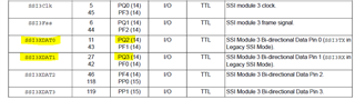
I have created a non RTOS version of the SPI loopback code in order to communicate between two TM4C1294XL boards , since im running in the default MOTO_MODE_0 , i believe i am running the SSI legacy mode which specifies that SSIXDAT0 behaves as the tx while SSIXDAT1 behaves as the rx. However since the general spi convention involves a mosi to mosi and miso to miso connection , i would like to know if there is anyway to swap these 2 lines . currently i am able to communicate between the two devices .

However for further development i would like to know how to swap these pins to allow me to connect to other test jigs and boards that follow the normal SPI convention .

i have attempted to change the functions assigned to each pin in the pin_map.h file in the ccs project , but this does not seem to change anything

#define GPIO_PQ2_SSI3XDAT0      0x000E080E        //   SSI3XDAT1      0x000E0C0E

#define GPIO_PQ3_SSI3XDAT1      0x000E0C0E       //   SSI3XDAT0      0x000E080E

             Original configuration                                          Desired configuration

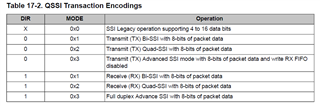
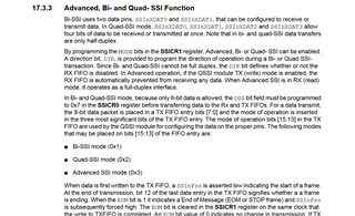
i have attempted to switch to SSIAdvMode with no success , can running the SSI in BI_READ and BI_WRITE solve my dilema

im willing to have simplex communication from master to Slave for one base and vice versa on another base


Stay safe and have a great day.

Best Regards,
William

  • Hi,

      This pin mapping is done at the hardware level. As you can see in the pin list, DATA0(TX) is mapped to PQ2 and DATA1(RX) is mapped to PQ3. There is no way to make PQ3 for TX and PQ2 for RX through a software change. 

  • Hi

    "is there any SSI mode we can use to send data from a SSIXDAT0 pin to a SSIXDAT0 pin on another base, essentially as it would be in the case of a MOSI or MISO line , unidirectionally"

    Best Regards,
    William

  • Hi,

      Sorry, that is not possible. SSIDAT0 is TX or acts as MOSI. You cannot make SSIDAT0 a RX(MISO). As explained, this pin mapping is done at the hardware level. You will need to connect SSIDAT0 from the MCU to MISO pin of a slave device.

  • Dear Tsai,

    The SSIXDAT0 is assigned as a TX in legacy mode , however is this the case universally for all the SSI mode including Bi-Read or Bi-Write or any other Advanced SSI mode

    Best Regards,
    William

  • Hi William,

      Please find below table about different SSI modes. Let's take Bi-SSI for example. In this mode, both SSIDAT0 and SSIDAT1 pins are used as TX pins. A 8-bit packet will use these two pins for transmission with each pin transmitting 4 bits of data. In another word, in Bi-SSI mode, there are only four SSI clock pulses. In Quad-SSI mode, All SSIDAT0, SSIDAT1, SSIDAT2, SSIDAT3 are used as TX pins. There are only two SSI clock pulses in this mode because each SSI clock pulse will clock out 4 bits of data at the same time. 

  • Dear Tsai,

    Kindly refer to the image below

    Best Regards,
    William

  • Hi William,

    #define GPIO_PQ2_SSI3XDAT0      0x000E080E        //   SSI3XDAT1      0x000E0C0E

    #define GPIO_PQ3_SSI3XDAT1      0x000E0C0E       //   SSI3XDAT0      0x000E080E

                 Original configuration                                          Desired configuration

    Sorry, I just got back from the vacation. I really don't know else to say. As I mentioned repeatedly, PQ2 is only for SSI3XDAT0. This connection is done by the hardware. You just cannot make PQ2 a SSI3XDAT1. 

    For Bi and Quad modes, PQ2 is still only for SSI3XDAT0 as shown in the datasheet. There is no way to make PQ3 for TX and PQ2 for RX through a software change. Please explain to this university student Aditya Bhardwaj as such.