This thread has been locked.

If you have a related question, please click the "Ask a related question" button in the top right corner. The newly created question will be automatically linked to this question.

MSP432E411Y-BGAEVM: EPI Bus GPIO pin change for SDRAM.

Part Number: MSP432E411Y-BGAEVM

Dear Team,

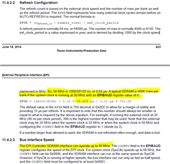
in our custom design of MSP432E401Y  SDRAM is connected with  EPI Bus interface. But there is single pin change when compared with given SDRAM example code of SDK.

The change are as follows:

1.Example code as following GPIO for EPIOS0

ROM_GPIOPinConfigure(GPIO_PH0_EPI0S0);

 2.Our custom design contains  GPIO for EPIOS0  

the changes i made as follows:

ROM_GPIOPinConfigure(GPIO_PK0_EPI0S0);

MAP_GPIOPinTypeEPI(GPIO_PORTK_BASE, (GPIO_PIN_5|GPIO_PIN_0));

3. What are changes need to done to make SDRAM work.

Regards,

Naga Narasimha Rao

  • Hi,

      I don't really see a problem mapping EPIOS0 to PK0 instead of PH0. I expect it to work. There is actually another SDRAM example for TM4C129 MCU that uses PK0 for EPIOS0 as well as other PKx for EPIOS[3:0]. You need to have SysCtlPeripheralEnable(SYSCTL_PERIPH_GPIOK) to enable port K which I suppose you already do. TM4C129 MCU is the same silicon as MSP432E4 but uses TivaWare SDK instead. 

    sdram.c
    //*****************************************************************************
    //
    // sdram.c - Example demonstrating how to configure the EPI bus in SDRAM
    //           mode.
    //
    // Copyright (c) 2014-2020 Texas Instruments Incorporated.  All rights reserved.
    // Software License Agreement
    // 
    //   Redistribution and use in source and binary forms, with or without
    //   modification, are permitted provided that the following conditions
    //   are met:
    // 
    //   Redistributions of source code must retain the above copyright
    //   notice, this list of conditions and the following disclaimer.
    // 
    //   Redistributions in binary form must reproduce the above copyright
    //   notice, this list of conditions and the following disclaimer in the
    //   documentation and/or other materials provided with the  
    //   distribution.
    // 
    //   Neither the name of Texas Instruments Incorporated nor the names of
    //   its contributors may be used to endorse or promote products derived
    //   from this software without specific prior written permission.
    // 
    // THIS SOFTWARE IS PROVIDED BY THE COPYRIGHT HOLDERS AND CONTRIBUTORS
    // "AS IS" AND ANY EXPRESS OR IMPLIED WARRANTIES, INCLUDING, BUT NOT
    // LIMITED TO, THE IMPLIED WARRANTIES OF MERCHANTABILITY AND FITNESS FOR
    // A PARTICULAR PURPOSE ARE DISCLAIMED. IN NO EVENT SHALL THE COPYRIGHT
    // OWNER OR CONTRIBUTORS BE LIABLE FOR ANY DIRECT, INDIRECT, INCIDENTAL,
    // SPECIAL, EXEMPLARY, OR CONSEQUENTIAL DAMAGES (INCLUDING, BUT NOT
    // LIMITED TO, PROCUREMENT OF SUBSTITUTE GOODS OR SERVICES; LOSS OF USE,
    // DATA, OR PROFITS; OR BUSINESS INTERRUPTION) HOWEVER CAUSED AND ON ANY
    // THEORY OF LIABILITY, WHETHER IN CONTRACT, STRICT LIABILITY, OR TORT
    // (INCLUDING NEGLIGENCE OR OTHERWISE) ARISING IN ANY WAY OUT OF THE USE
    // OF THIS SOFTWARE, EVEN IF ADVISED OF THE POSSIBILITY OF SUCH DAMAGE.
    // 
    // This is part of revision 2.2.0.295 of the Tiva Firmware Development Package.
    //
    //*****************************************************************************
    
    #include <stdbool.h>
    #include <stdint.h>
    #include "inc/hw_epi.h"
    #include "inc/hw_memmap.h"
    #include "inc/hw_types.h"
    #include "inc/hw_gpio.h"
    #include "driverlib/epi.h"
    #include "driverlib/gpio.h"
    #include "driverlib/pin_map.h"
    #include "driverlib/sysctl.h"
    #include "driverlib/uart.h"
    #include "utils/uartstdio.h"
    
    //*****************************************************************************
    //
    //! \addtogroup epi_examples_list
    //! <h1>EPI SDRAM Mode (sdram)</h1>
    //!
    //! This example shows how to configure the TM4C129 EPI bus in SDRAM mode.  It
    //! assumes that a 64Mbit SDRAM is attached to EPI0.
    //!
    //! For the EPI SDRAM mode, the pinout is as follows:
    //!     Address11:0 - EPI0S11:0
    //!     Bank1:0     - EPI0S14:13
    //!     Data15:0    - EPI0S15:0
    //!     DQML        - EPI0S16
    //!     DQMH        - EPI0S17
    //!     /CAS        - EPI0S18
    //!     /RAS        - EPI0S19
    //!     /WE         - EPI0S28
    //!     /CS         - EPI0S29
    //!     SDCKE       - EPI0S30
    //!     SDCLK       - EPI0S31
    //!
    //! This example uses the following peripherals and I/O signals.  You must
    //! review these and change as needed for your own board:
    //! - EPI0 peripheral
    //! - GPIO Port A peripheral (for EPI0 pins)
    //! - GPIO Port B peripheral (for EPI0 pins)
    //! - GPIO Port C peripheral (for EPI0 pins)
    //! - GPIO Port G peripheral (for EPI0 pins)
    //! - GPIO Port K peripheral (for EPI0 pins)
    //! - GPIO Port L peripheral (for EPI0 pins)
    //! - GPIO Port M peripheral (for EPI0 pins)
    //! - GPIO Port N peripheral (for EPI0 pins)
    //! - EPI0S0  - PK0
    //! - EPI0S1  - PK1
    //! - EPI0S2  - PK2
    //! - EPI0S3  - PK3
    //! - EPI0S4  - PC7
    //! - EPI0S5  - PC6
    //! - EPI0S6  - PC5
    //! - EPI0S7  - PC4
    //! - EPI0S8  - PA6
    //! - EPI0S9  - PA7
    //! - EPI0S10 - PG1
    //! - EPI0S11 - PG0
    //! - EPI0S12 - PM3
    //! - EPI0S13 - PM2
    //! - EPI0S14 - PM1
    //! - EPI0S15 - PM0
    //! - EPI0S16 - PL0
    //! - EPI0S17 - PL1
    //! - EPI0S18 - PL2
    //! - EPI0S19 - PL3
    //! - EPI0S28 - PB3
    //! - EPI0S29 - PN2
    //! - EPI0S30 - PN3
    //! - EPI0S31 - PK5
    //!
    //! The following UART signals are configured only for displaying console
    //! messages for this example.  These are not required for operation of EPI0.
    //! - UART0 peripheral
    //! - GPIO Port A peripheral (for UART0 pins)
    //! - UART0RX - PA0
    //! - UART0TX - PA1
    //!
    //! This example uses the following interrupt handlers.  To use this example
    //! in your own application you must add these interrupt handlers to your
    //! vector table.
    //! - None.
    //
    //*****************************************************************************
    
    //*****************************************************************************
    //
    // Use the following to specify the GPIO pins used by the SDRAM EPI bus.
    //
    //*****************************************************************************
    #define EPI_PORTA_PINS (GPIO_PIN_7 | GPIO_PIN_6)
    #define EPI_PORTB_PINS (GPIO_PIN_3)
    #define EPI_PORTC_PINS (GPIO_PIN_7 | GPIO_PIN_6 | GPIO_PIN_5 | GPIO_PIN_4)
    #define EPI_PORTG_PINS (GPIO_PIN_1 | GPIO_PIN_0)
    #define EPI_PORTK_PINS (GPIO_PIN_5 | GPIO_PIN_3 | GPIO_PIN_2 | GPIO_PIN_1 |   \
                            GPIO_PIN_0)
    #define EPI_PORTL_PINS (GPIO_PIN_3 | GPIO_PIN_2 | GPIO_PIN_1 | GPIO_PIN_0)
    #define EPI_PORTM_PINS (GPIO_PIN_3 | GPIO_PIN_2 | GPIO_PIN_1 | GPIO_PIN_0)
    #define EPI_PORTN_PINS (GPIO_PIN_3 | GPIO_PIN_2)
    
    //*****************************************************************************
    //
    // The starting and ending address for the 64MB SDRAM chip (32Meg x 16bits) on
    // the SDRAM daughter board.
    //
    //*****************************************************************************
    #define SDRAM_START_ADDRESS 0x00000000
    #define SDRAM_END_ADDRESS   0x01FFFFFF
    
    //*****************************************************************************
    //
    // The Mapping address space for the EPI SDRAM.
    //
    //*****************************************************************************
    #define SDRAM_MAPPING_ADDRESS 0x60000000
    
    //*****************************************************************************
    //
    // A pointer to the EPI memory aperture.  Note that g_pui16EPISdram is declared
    // as volatile so the compiler should not optimize reads out of the image.
    //
    //*****************************************************************************
    static volatile uint16_t *g_pui16EPISdram;
    
    //*****************************************************************************
    //
    // A table used to determine the EPI clock frequency band in use.
    //
    //*****************************************************************************
    typedef struct
    {
        uint32_t ui32SysClock;
        uint32_t ui32FreqFlag;
    }
    tSDRAMFreqMapping;
    
    static tSDRAMFreqMapping g_psSDRAMFreq[] =
    {
        //
        // SysClock >= 100MHz, EPI clock >= 50Mhz (divided by 2)
        //
        {100000000, EPI_SDRAM_CORE_FREQ_50_100},
    
        //
        // SysClock >= 60MHz, EPI clock >= 30MHz (divided by 2)
        //
        {60000000, EPI_SDRAM_CORE_FREQ_50_100},
    
        //
        // SysClock >= 50MHz, EPI clock >= 50MHz (no divider)
        //
        {50000000, EPI_SDRAM_CORE_FREQ_50_100},
    
        //
        // SysClock >= 30MHz, EPI clock >= 30MHz (no divider)
        //
        {50000000, EPI_SDRAM_CORE_FREQ_30_50},
    
        //
        // SysClock >= 15MHz, EPI clock >= 15MHz (no divider)
        //
        {15000000, EPI_SDRAM_CORE_FREQ_15_30},
    
        //
        // SysClock < 15Mhz, EPI clock < 15Mhz (no divider)
        //
        {0, EPI_SDRAM_CORE_FREQ_0_15}
     };
    
    #define NUM_SDRAM_FREQ (sizeof(g_psSDRAMFreq) / sizeof(tSDRAMFreqMapping))
    
    //*****************************************************************************
    //
    // This function sets up UART0 to be used for a console to display information
    // as the example is running.
    //
    //*****************************************************************************
    void
    InitConsole(void)
    {
        //
        // Enable GPIO port A which is used for UART0 pins.
        // TODO: change this to whichever GPIO port you are using.
        //
        SysCtlPeripheralEnable(SYSCTL_PERIPH_GPIOA);
    
        //
        // Configure the pin muxing for UART0 functions on port A0 and A1.
        // This step is not necessary if your part does not support pin muxing.
        // TODO: change this to select the port/pin you are using.
        //
        GPIOPinConfigure(GPIO_PA0_U0RX);
        GPIOPinConfigure(GPIO_PA1_U0TX);
    
        //
        // Enable UART0 so that we can configure the clock.
        //
        SysCtlPeripheralEnable(SYSCTL_PERIPH_UART0);
    
        //
        // Use the internal 16MHz oscillator as the UART clock source.
        //
        UARTClockSourceSet(UART0_BASE, UART_CLOCK_PIOSC);
    
        //
        // Select the alternate (UART) function for these pins.
        // TODO: change this to select the port/pin you are using.
        //
        GPIOPinTypeUART(GPIO_PORTA_BASE, GPIO_PIN_0 | GPIO_PIN_1);
    
        //
        // Initialize the UART for console I/O.
        //
        UARTStdioConfig(0, 115200, 16000000);
    }
    
    //*****************************************************************************
    //
    // Configure EPI0 in SDRAM mode.  The EPI memory space is setup using an a
    // simple C array.  This example shows how to read and write to an SDRAM card
    // using the EPI bus in SDRAM mode.
    //
    //*****************************************************************************
    int
    main(void)
    {
        uint32_t ui32Val, ui32Freq, ui32SysClock;
    
        //
        // Set the clocking to run at 120MHz from the PLL.
        // TODO: Update this call to set the system clock frequency your
        // application requires.
        //
        ui32SysClock = SysCtlClockFreqSet((SYSCTL_OSC_INT | SYSCTL_USE_PLL |
                                          SYSCTL_CFG_VCO_320), 120000000);
    
        //
        // Set up the serial console to use for displaying messages.  This is
        // just for this example program and is not needed for EPI operation.
        //
        InitConsole();
    
        //
        // Display the setup on the console.
        //
        UARTprintf("EPI SDRAM Mode ->\n");
        UARTprintf("  Type: SDRAM\n");
        UARTprintf("  Starting Address: 0x%08x\n", SDRAM_MAPPING_ADDRESS);
        UARTprintf("  End Address: 0x%08x\n",
                   (SDRAM_MAPPING_ADDRESS + SDRAM_END_ADDRESS));
        UARTprintf("  Data: 16-bit\n");
        UARTprintf("  Size: 64MB (32Meg x 16bits)\n\n");
    
        //
        // The EPI0 peripheral must be enabled for use.
        //
        SysCtlPeripheralEnable(SYSCTL_PERIPH_EPI0);
    
        //
        // For this example EPI0 is used with multiple pins on PortA, B, C, G, H,
        // K, L, M and N.  The actual port and pins used may be different on your
        // part, consult the data sheet for more information.
        // TODO: Update based upon the EPI pin assignment on your target part.
        //
        SysCtlPeripheralEnable(SYSCTL_PERIPH_GPIOA);
        SysCtlPeripheralEnable(SYSCTL_PERIPH_GPIOB);
        SysCtlPeripheralEnable(SYSCTL_PERIPH_GPIOC);
        SysCtlPeripheralEnable(SYSCTL_PERIPH_GPIOG);
        SysCtlPeripheralEnable(SYSCTL_PERIPH_GPIOK);
        SysCtlPeripheralEnable(SYSCTL_PERIPH_GPIOL);
        SysCtlPeripheralEnable(SYSCTL_PERIPH_GPIOM);
        SysCtlPeripheralEnable(SYSCTL_PERIPH_GPION);
    
        //
        // This step configures the internal pin muxes to set the EPI pins for use
        // with EPI.  Please refer to the datasheet for more information about pin
        // muxing.  Note that EPI0S27:20 are not used for the EPI SDRAM
        // implementation.
        // TODO: Update this section based upon the EPI pin assignment on your
        // target part.
        //
    
        //
        // EPI0S4 ~ EPI0S7: C4 ~ 7
        //
        ui32Val = HWREG(GPIO_PORTC_BASE + GPIO_O_PCTL);
        ui32Val &= 0x0000FFFF;
        ui32Val |= 0xFFFF0000;
        HWREG(GPIO_PORTC_BASE + GPIO_O_PCTL) = ui32Val;
    
        //
        // EPI0S8 ~ EPI0S9: A6 ~ 7
        //
        ui32Val = HWREG(GPIO_PORTA_BASE + GPIO_O_PCTL);
        ui32Val &= 0x00FFFFFF;
        ui32Val |= 0xFF000000;
        HWREG(GPIO_PORTA_BASE + GPIO_O_PCTL) = ui32Val;
    
        //
        // EPI0S10 ~ EPI0S11: G0 ~ 1
        //
        ui32Val = HWREG(GPIO_PORTG_BASE + GPIO_O_PCTL);
        ui32Val &= 0xFFFFFF00;
        ui32Val |= 0x000000FF;
        HWREG(GPIO_PORTG_BASE + GPIO_O_PCTL) = ui32Val;
    
        //
        // EPI0S12 ~ EPI0S15: M0 ~ 3
        //
        ui32Val = HWREG(GPIO_PORTM_BASE + GPIO_O_PCTL);
        ui32Val &= 0xFFFF0000;
        ui32Val |= 0x0000FFFF;
        HWREG(GPIO_PORTM_BASE + GPIO_O_PCTL) = ui32Val;
    
        //
        // EPI0S16 ~ EPI0S19: L0 ~ 3
        //
        ui32Val = HWREG(GPIO_PORTL_BASE + GPIO_O_PCTL);
        ui32Val &= 0xFFFF0000;
        ui32Val |= 0x0000FFFF;
        HWREG(GPIO_PORTL_BASE + GPIO_O_PCTL) = ui32Val;
    
        //
        // EPI0S28 : B3
        //
        ui32Val = HWREG(GPIO_PORTB_BASE + GPIO_O_PCTL);
        ui32Val &= 0xFFFF0FFF;
        ui32Val |= 0x0000F000;
        HWREG(GPIO_PORTB_BASE + GPIO_O_PCTL) = ui32Val;
    
        //
        // EPI0S29 ~ EPI0S30: N2 ~ 3
        //
        ui32Val = HWREG(GPIO_PORTN_BASE + GPIO_O_PCTL);
        ui32Val &= 0xFFFF00FF;
        ui32Val |= 0x0000FF00;
        HWREG(GPIO_PORTN_BASE + GPIO_O_PCTL) = ui32Val;
    
        //
        // EPI0S00 ~ EPI0S03, EPI0S31 : K0 ~ 3, K5
        //
        ui32Val = HWREG(GPIO_PORTK_BASE + GPIO_O_PCTL);
        ui32Val &= 0xFF0F0000;
        ui32Val |= 0x00F0FFFF;
        HWREG(GPIO_PORTK_BASE + GPIO_O_PCTL) = ui32Val;
    
        //
        // Configure the GPIO pins for EPI mode.  All the EPI pins require 8mA
        // drive strength in push-pull operation.  This step also gives control of
        // pins to the EPI module.
        //
        GPIOPinTypeEPI(GPIO_PORTA_BASE, EPI_PORTA_PINS);
        GPIOPinTypeEPI(GPIO_PORTB_BASE, EPI_PORTB_PINS);
        GPIOPinTypeEPI(GPIO_PORTC_BASE, EPI_PORTC_PINS);
        GPIOPinTypeEPI(GPIO_PORTG_BASE, EPI_PORTG_PINS);
        GPIOPinTypeEPI(GPIO_PORTK_BASE, EPI_PORTK_PINS);
        GPIOPinTypeEPI(GPIO_PORTL_BASE, EPI_PORTL_PINS);
        GPIOPinTypeEPI(GPIO_PORTM_BASE, EPI_PORTM_PINS);
        GPIOPinTypeEPI(GPIO_PORTN_BASE, EPI_PORTN_PINS);
    
        //
        // Is our current system clock faster than we can drive the SDRAM clock?
        //
        if(ui32SysClock > 60000000)
        {
            //
            // Yes. Set the EPI clock to half the system clock.
            //
            EPIDividerSet(EPI0_BASE, 1);
        }
        else
        {
            //
            // With a system clock of 60MHz or lower, we can drive the SDRAM at
            // the same rate so set the divider to 0.
            //
            EPIDividerSet(EPI0_BASE, 0);
        }
    
        //
        // Sets the usage mode of the EPI module.  For this example we will use
        // the SDRAM mode to talk to the external 64MB SDRAM daughter card.
        //
        EPIModeSet(EPI0_BASE, EPI_MODE_SDRAM);
    
        //
        // Keep the compiler happy by setting a default value for the frequency
        // flag.
        //
        ui32Freq = g_psSDRAMFreq[NUM_SDRAM_FREQ - 1].ui32FreqFlag;
    
        //
        // Examine the system clock frequency to determine how to set the SDRAM
        // controller's frequency flag.
        //
        for(ui32Val = 0; ui32Val < NUM_SDRAM_FREQ; ui32Val++)
        {
            //
            // Is the system clock frequency above the break point in the table?
            //
            if(ui32SysClock >= g_psSDRAMFreq[ui32Val].ui32SysClock)
            {
                //
                // Yes - remember the frequency flag to use and exit the loop.
                //
                ui32Freq = g_psSDRAMFreq[ui32Val].ui32FreqFlag;
                break;
            }
        }
    
        //
        // Configure the SDRAM mode.  We configure the SDRAM according to our core
        // clock frequency.  We will use the normal (or full power) operating
        // state which means we will not use the low power self-refresh state.
        // Set the SDRAM size to 64MB with a refresh interval of 1024 clock ticks.
        //
        EPIConfigSDRAMSet(EPI0_BASE, (ui32Freq | EPI_SDRAM_FULL_POWER |
                          EPI_SDRAM_SIZE_512MBIT), 1024);
    
        //
        // Set the address map.  The EPI0 is mapped from 0x60000000 to 0x01FFFFFF.
        // For this example, we will start from a base address of 0x60000000 with
        // a size of 256MB.  Although our SDRAM is only 64MB, there is no 64MB
        // aperture option so we pick the next larger size.
        //
        EPIAddressMapSet(EPI0_BASE, EPI_ADDR_RAM_SIZE_256MB | EPI_ADDR_RAM_BASE_6);
    
        //
        // Wait for the SDRAM wake-up to complete by polling the SDRAM
        // initialization sequence bit.  This bit is true when the SDRAM interface
        // is going through the initialization and false when the SDRAM interface
        // it is not in a wake-up period.
        //
        while(HWREG(EPI0_BASE + EPI_O_STAT) &  EPI_STAT_INITSEQ)
        {
        }
    
        //
        // Set the EPI memory pointer to the base of EPI memory space.  Note that
        // g_pui16EPISdram is declared as volatile so the compiler should not
        // optimize reads out of the memory.  With this pointer, the memory space
        // is accessed like a simple array.
        //
        g_pui16EPISdram = (uint16_t *)0x60000000;
    
        //
        // Read the initial data in SDRAM, and display it on the console.
        //
        UARTprintf("  SDRAM Initial Data:\n");
        UARTprintf("     Mem[0x6000.0000] = 0x%4x\n",
                   g_pui16EPISdram[SDRAM_START_ADDRESS]);
        UARTprintf("     Mem[0x6000.0001] = 0x%4x\n",
                   g_pui16EPISdram[SDRAM_START_ADDRESS + 1]);
        UARTprintf("     Mem[0x603F.FFFE] = 0x%4x\n",
                   g_pui16EPISdram[SDRAM_END_ADDRESS - 1]);
        UARTprintf("     Mem[0x603F.FFFF] = 0x%4x\n\n",
                   g_pui16EPISdram[SDRAM_END_ADDRESS]);
    
        //
        // Display what writes we are doing on the console.
        //
        UARTprintf("  SDRAM Write:\n");
        UARTprintf("     Mem[0x6000.0000] <- 0xabcd\n");
        UARTprintf("     Mem[0x6000.0001] <- 0x1234\n");
        UARTprintf("     Mem[0x603F.FFFE] <- 0xdcba\n");
        UARTprintf("     Mem[0x603F.FFFF] <- 0x4321\n\n");
    
        //
        // Write to the first 2 and last 2 address of the SDRAM card.  Since the
        // SDRAM card is word addressable, we will write words.
        //
        g_pui16EPISdram[SDRAM_START_ADDRESS] = 0xabcd;
        g_pui16EPISdram[SDRAM_START_ADDRESS + 1] = 0x1234;
        g_pui16EPISdram[SDRAM_END_ADDRESS - 1] = 0xdcba;
        g_pui16EPISdram[SDRAM_END_ADDRESS] = 0x4321;
    
        //
        // Read back the data you wrote, and display it on the console.
        //
        UARTprintf("  SDRAM Read:\n");
        UARTprintf("     Mem[0x6000.0000] = 0x%4x\n",
                   g_pui16EPISdram[SDRAM_START_ADDRESS]);
        UARTprintf("     Mem[0x6000.0001] = 0x%4x\n",
                   g_pui16EPISdram[SDRAM_START_ADDRESS + 1]);
        UARTprintf("     Mem[0x603F.FFFE] = 0x%4x\n",
                   g_pui16EPISdram[SDRAM_END_ADDRESS - 1]);
        UARTprintf("     Mem[0x603F.FFFF] = 0x%4x\n\n",
                   g_pui16EPISdram[SDRAM_END_ADDRESS]);
    
        //
        // Check the validity of the data.
        //
        if((g_pui16EPISdram[SDRAM_START_ADDRESS] == 0xabcd) &&
           (g_pui16EPISdram[SDRAM_START_ADDRESS + 1] == 0x1234) &&
           (g_pui16EPISdram[SDRAM_END_ADDRESS - 1] == 0xdcba) &&
           (g_pui16EPISdram[SDRAM_END_ADDRESS] == 0x4321))
        {
            //
            // Read and write operations were successful.  Return with no errors.
            //
            UARTprintf("Read and write to external SDRAM was successful!\n");
            return(0);
        }
    
        //
        // Display on the console that there was an error.
        //
        UARTprintf("Read and/or write failure!");
        UARTprintf(" Check if your SDRAM card is plugged in.");
    
        //
        // Read and/or write operations were unsuccessful.  Wait in while(1) loop
        // for debugging.
        //
        while(1)
        {
        }
    }
    

  • /* --COPYRIGHT--,BSD
    * Copyright (c) 2017, Texas Instruments Incorporated
    * All rights reserved.
    *
    * Redistribution and use in source and binary forms, with or without
    * modification, are permitted provided that the following conditions
    * are met:
    *
    * * Redistributions of source code must retain the above copyright
    * notice, this list of conditions and the following disclaimer.
    *
    * * Redistributions in binary form must reproduce the above copyright
    * notice, this list of conditions and the following disclaimer in the
    * documentation and/or other materials provided with the distribution.
    *
    * * Neither the name of Texas Instruments Incorporated nor the names of
    * its contributors may be used to endorse or promote products derived
    * from this software without specific prior written permission.
    *
    * THIS SOFTWARE IS PROVIDED BY THE COPYRIGHT HOLDERS AND CONTRIBUTORS "AS IS"
    * AND ANY EXPRESS OR IMPLIED WARRANTIES, INCLUDING, BUT NOT LIMITED TO,
    * THE IMPLIED WARRANTIES OF MERCHANTABILITY AND FITNESS FOR A PARTICULAR
    * PURPOSE ARE DISCLAIMED. IN NO EVENT SHALL THE COPYRIGHT OWNER OR
    * CONTRIBUTORS BE LIABLE FOR ANY DIRECT, INDIRECT, INCIDENTAL, SPECIAL,
    * EXEMPLARY, OR CONSEQUENTIAL DAMAGES (INCLUDING, BUT NOT LIMITED TO,
    * PROCUREMENT OF SUBSTITUTE GOODS OR SERVICES; LOSS OF USE, DATA, OR PROFITS;
    * OR BUSINESS INTERRUPTION) HOWEVER CAUSED AND ON ANY THEORY OF LIABILITY,
    * WHETHER IN CONTRACT, STRICT LIABILITY, OR TORT (INCLUDING NEGLIGENCE OR
    * OTHERWISE) ARISING IN ANY WAY OUT OF THE USE OF THIS SOFTWARE,
    * EVEN IF ADVISED OF THE POSSIBILITY OF SUCH DAMAGE.
    * --/COPYRIGHT--*/
    /******************************************************************************
    * MSP432E4 example code for EPI to access SDRAM memory using DMA.
    *
    * Description: The EPI is configured to access an SDRAM memory at 60MHz. The
    * example programs the GPIOs for EPI and configures the EPI. After the
    * initialization is complete, the EPI is configured to generate a DMA TX
    * request to write an internal buffer to the SDRAM memory. On completion the
    * non-blocking read FIFO is configured to read the data from the SDRAM to
    * another internal buffer. The resulting data check is printed on the console
    * along with the throughput.
    *
    * MSP432E401Y
    * ------------------
    * /|\| |
    * | | |
    * --|RST EPI|-->SDRAM
    * | |
    * | |
    * | |
    * | PA0|<--U0RX
    * | PA1|-->U0TX
    * Author: Amit Ashara
    *******************************************************************************/
    /* DriverLib Includes */
    #include <ti/devices/msp432e4/driverlib/driverlib.h>

    /* Standard Includes */
    #include <stdint.h>
    #include <stdlib.h>
    #include <stdbool.h>

    /* Display Include via console */
    #include "uartstdio.h"

    /* Defines for the scope of the example */
    #define SDRAM_START_ADDRESS 0x00000000
    #define SDRAM_END_ADDRESS 0x01FFFFFF
    #define NO_OF_RAM_LOC 512
    #define SDRAM_MAPPING_ADDRESS 0x60000000
    #define SYSTICK_MAX_COUNT 16777216

    /* The control table used by the uDMA controller. This table must be aligned
    * to a 1024 byte boundary. */
    #if defined(__ICCARM__)
    #pragma data_alignment=1024
    uint8_t pui8ControlTable[1024];
    #elif defined(__TI_ARM__)
    #pragma DATA_ALIGN(pui8ControlTable, 1024)
    uint8_t pui8ControlTable[1024];
    #else
    uint8_t pui8ControlTable[1024] __attribute__ ((aligned(1024)));
    #endif

    /* Global Variables */
    uint32_t internalWriteBuf[NO_OF_RAM_LOC];
    uint32_t internalReadBuf[NO_OF_RAM_LOC];
    bool setTransmitDone = false;
    bool setReceiveDone = false;

    void EPI0_IRQHandler(void)
    {
    uint32_t getIntStatus;

    /* Get the interrupt status */
    getIntStatus = MAP_EPIIntStatus(EPI0_BASE, true);

    if((getIntStatus & EPI_INT_DMA_TX_DONE) == EPI_INT_DMA_TX_DONE)
    {
    /* Clear the interrupt status and set the flag for the main code to
    * proceed */
    MAP_EPIIntErrorClear(EPI0_BASE, EPI_INT_ERR_DMAWRIC);
    setTransmitDone = true;
    }

    if((getIntStatus & EPI_INT_DMA_RX_DONE) == EPI_INT_DMA_RX_DONE)
    {
    /* Clear the interrupt status and set the flag for the main code to
    * proceed */
    MAP_EPIIntErrorClear(EPI0_BASE, EPI_INT_ERR_DMARDIC);
    setReceiveDone = true;
    }

    }

    void ConfigureUART(uint32_t systemClock)
    {
    /* Enable the clock to GPIO port A and UART 0 */
    MAP_SysCtlPeripheralEnable(SYSCTL_PERIPH_GPIOA);
    MAP_SysCtlPeripheralEnable(SYSCTL_PERIPH_UART0);

    /* Configure the GPIO Port A for UART 0 */
    MAP_GPIOPinConfigure(GPIO_PA0_U0RX);
    MAP_GPIOPinConfigure(GPIO_PA1_U0TX);
    MAP_GPIOPinTypeUART(GPIO_PORTA_BASE, GPIO_PIN_0 | GPIO_PIN_1);

    /* Configure the UART for 115200 bps 8-N-1 format */
    UARTStdioConfig(0, 115200, systemClock);
    }

    int main(void)
    {
    uint32_t systemClock;
    uint32_t ii;
    uint32_t getStartTime, getEndTime;
    uint32_t systemClockinMHz;
    uint32_t *sdram32bitAddrPointer;
    bool setDataCheck = false;

    /* Configure the system clock for 120 MHz */
    systemClock = MAP_SysCtlClockFreqSet((SYSCTL_XTAL_25MHZ | SYSCTL_OSC_MAIN |
    SYSCTL_USE_PLL | SYSCTL_CFG_VCO_480),
    120000000);

    /* Initialize serial console */
    ConfigureUART(systemClock);

    /* Enable the clock to the GPIO Ports that are required for EPI */
    MAP_SysCtlPeripheralEnable(SYSCTL_PERIPH_GPIOA);
    MAP_SysCtlPeripheralEnable(SYSCTL_PERIPH_GPIOB);
    MAP_SysCtlPeripheralEnable(SYSCTL_PERIPH_GPIOC);
    MAP_SysCtlPeripheralEnable(SYSCTL_PERIPH_GPIOG);
    MAP_SysCtlPeripheralEnable(SYSCTL_PERIPH_GPIOH);
    MAP_SysCtlPeripheralEnable(SYSCTL_PERIPH_GPIOK);
    MAP_SysCtlPeripheralEnable(SYSCTL_PERIPH_GPIOL);
    MAP_SysCtlPeripheralEnable(SYSCTL_PERIPH_GPIOM);
    MAP_SysCtlPeripheralEnable(SYSCTL_PERIPH_GPIOP);

    MAP_GPIOPinConfigure(GPIO_PH0_EPI0S0); 
    MAP_GPIOPinConfigure(GPIO_PH1_EPI0S1);
    MAP_GPIOPinConfigure(GPIO_PH2_EPI0S2);
    MAP_GPIOPinConfigure(GPIO_PH3_EPI0S3);
    MAP_GPIOPinConfigure(GPIO_PC7_EPI0S4);
    MAP_GPIOPinConfigure(GPIO_PC6_EPI0S5);
    MAP_GPIOPinConfigure(GPIO_PC5_EPI0S6);
    MAP_GPIOPinConfigure(GPIO_PC4_EPI0S7);
    MAP_GPIOPinConfigure(GPIO_PA6_EPI0S8);
    MAP_GPIOPinConfigure(GPIO_PA7_EPI0S9);
    MAP_GPIOPinConfigure(GPIO_PG1_EPI0S10);
    MAP_GPIOPinConfigure(GPIO_PG0_EPI0S11);
    MAP_GPIOPinConfigure(GPIO_PM3_EPI0S12);
    MAP_GPIOPinConfigure(GPIO_PM2_EPI0S13);
    MAP_GPIOPinConfigure(GPIO_PM1_EPI0S14);
    MAP_GPIOPinConfigure(GPIO_PM0_EPI0S15);
    MAP_GPIOPinConfigure(GPIO_PL0_EPI0S16);
    MAP_GPIOPinConfigure(GPIO_PL1_EPI0S17);
    MAP_GPIOPinConfigure(GPIO_PL2_EPI0S18);
    MAP_GPIOPinConfigure(GPIO_PL3_EPI0S19);
    MAP_GPIOPinConfigure(GPIO_PB3_EPI0S28);
    MAP_GPIOPinConfigure(GPIO_PP2_EPI0S29);
    MAP_GPIOPinConfigure(GPIO_PP3_EPI0S30);
    MAP_GPIOPinConfigure(GPIO_PK5_EPI0S31);

    MAP_GPIOPinTypeEPI(GPIO_PORTA_BASE, (GPIO_PIN_7 | GPIO_PIN_6));
    MAP_GPIOPinTypeEPI(GPIO_PORTB_BASE, (GPIO_PIN_3));
    MAP_GPIOPinTypeEPI(GPIO_PORTC_BASE, (GPIO_PIN_7 | GPIO_PIN_6 | GPIO_PIN_5 |
    GPIO_PIN_4));
    MAP_GPIOPinTypeEPI(GPIO_PORTG_BASE, (GPIO_PIN_1 | GPIO_PIN_0));
    MAP_GPIOPinTypeEPI(GPIO_PORTH_BASE, (GPIO_PIN_3 | GPIO_PIN_2 | GPIO_PIN_1 |
    GPIO_PIN_0));
    MAP_GPIOPinTypeEPI(GPIO_PORTK_BASE, (GPIO_PIN_5));
    MAP_GPIOPinTypeEPI(GPIO_PORTL_BASE, (GPIO_PIN_3 | GPIO_PIN_2 | GPIO_PIN_1 |
    GPIO_PIN_0));
    MAP_GPIOPinTypeEPI(GPIO_PORTM_BASE, (GPIO_PIN_3 | GPIO_PIN_2 | GPIO_PIN_1 |
    GPIO_PIN_0));
    MAP_GPIOPinTypeEPI(GPIO_PORTP_BASE, (GPIO_PIN_3 | GPIO_PIN_2));

    /* Enable the clock to the EPI and wait for it to be ready */
    MAP_SysCtlPeripheralEnable(SYSCTL_PERIPH_EPI0);
    while(!(MAP_SysCtlPeripheralReady(SYSCTL_PERIPH_EPI0)))
    {
    }

    /* Configure the EPI to access the SDRAM memory at 60 MHz Set the EPI
    * clock to half the system clock. */
    MAP_EPIDividerSet(EPI0_BASE, 1);

    /* Sets the usage mode of the EPI module. For this example we will use
    * the SDRAM mode to talk to the external 64MB SDRAM daughter card. */
    MAP_EPIModeSet(EPI0_BASE, EPI_MODE_SDRAM);

    /* Configure the SDRAM mode. We configure the SDRAM according to our core
    * clock frequency. We will use the normal (or full power) operating
    * state which means we will not use the low power self-refresh state.
    * Set the SDRAM size to 64MB with a refresh interval of 468 clock ticks*/
    MAP_EPIConfigSDRAMSet(EPI0_BASE, (EPI_SDRAM_CORE_FREQ_50_100 |
    EPI_SDRAM_FULL_POWER |
    EPI_SDRAM_SIZE_512MBIT), 468);

    /* Set the address map. The EPI0 is mapped from 0x60000000 to 0x01FFFFFF.
    * For this example, we will start from a base address of 0x60000000 with
    * a size of 256MB. Although our SDRAM is only 64MB, there is no 64MB
    * aperture option so we pick the next larger size. */
    MAP_EPIAddressMapSet(EPI0_BASE, EPI_ADDR_RAM_SIZE_256MB | EPI_ADDR_RAM_BASE_6);

    /* Wait for the SDRAM wake-up to complete by polling the SDRAM
    * initialization sequence bit. This bit is true when the SDRAM interface
    * is going through the initialization and false when the SDRAM interface
    * it is not in a wake-up period. */
    while(EPI0->STAT & EPI_STAT_INITSEQ)
    {
    }

    /* Set the EPI memory pointer to the base of EPI memory space. Note that
    * sdram32bitAddrPointer is declared as volatile so the compiler should not
    * optimize reads out of the memory. With this pointer, the memory space
    * is accessed like a simple array. */
    sdram32bitAddrPointer = (uint32_t *)SDRAM_MAPPING_ADDRESS;

    /* Read the initial data in SDRAM, and display it on the console. */
    UARTprintf(" SDRAM Initial Data:\n");
    UARTprintf(" Mem[0x6000.0000] = 0x%8x\n",
    sdram32bitAddrPointer[SDRAM_START_ADDRESS]);
    UARTprintf(" Mem[0x603F.FFFF] = 0x%8x\n\n",
    sdram32bitAddrPointer[SDRAM_END_ADDRESS]);

    /* Display what writes we are doing on the console. */
    UARTprintf(" SDRAM Write:\n");
    UARTprintf(" Mem[0x6000.0000] <- 0xabcd1234\n");
    UARTprintf(" Mem[0x603F.FFFF] <- 0x4321dcba\n\n");

    /* Write to the first 2 and last 2 address of the SDRAM card. Since the
    * SDRAM card is word addressable, we will write words. */
    sdram32bitAddrPointer[SDRAM_START_ADDRESS] = 0xabcd1234;
    sdram32bitAddrPointer[SDRAM_END_ADDRESS] = 0x4321dcba;

    /* Read back the data you wrote, and display it on the console. */
    UARTprintf(" SDRAM Read:\n");
    UARTprintf(" Mem[0x6000.0000] = 0x%8x\n",
    sdram32bitAddrPointer[SDRAM_START_ADDRESS]);
    UARTprintf(" Mem[0x603F.FFFF] = 0x%8x\n\n",
    sdram32bitAddrPointer[SDRAM_END_ADDRESS]);

    /* Check the integrity of the data. */
    if((sdram32bitAddrPointer[SDRAM_START_ADDRESS] == 0xabcd1234) &&
    (sdram32bitAddrPointer[SDRAM_END_ADDRESS] == 0x4321dcba))
    {
    /* Read and write operations were successful. Return with no errors.
    * */
    UARTprintf("Read and write to external SDRAM was successful!\n");
    UARTprintf("Begin Performance Test!\n");
    }
    else
    {
    /* Display on the console that there was an error. */
    UARTprintf("Read and/or write failure!");
    UARTprintf(" Check if your SDRAM card is plugged in.");
    return(0);
    }

    /* Update the internal write buffer with random data and clear the internal
    * read buffer */
    for(ii = 0; ii < NO_OF_RAM_LOC; ii++)
    {
    internalWriteBuf[ii] = rand() | (rand() << 16);
    internalReadBuf[ii] = 0x0;
    }

    /* Configure the Write and Read Path DMA Request for EPI. The TX FIFO is
    * configured to generate a request when there are 2 locations available.
    * The RX FIFO is configured when the NBR FIFO is Half Full with 4 words.*/
    MAP_EPIFIFOConfig(EPI0_BASE, EPI_FIFO_CONFIG_TX_1_4 |
    EPI_FIFO_CONFIG_RX_1_2);

    MAP_EPINonBlockingReadConfigure(EPI0_BASE, 0, EPI_NBCONFIG_SIZE_32,
    0x60000000);

    MAP_EPIIntEnable(EPI0_BASE, (EPI_INT_DMA_TX_DONE | EPI_INT_DMA_RX_DONE));

    MAP_IntEnable(INT_EPI0);

    /* Enable the DMA and Configure Channel for EPI TX and RX in BASIC mode of
    * transfer */
    MAP_SysCtlPeripheralEnable(SYSCTL_PERIPH_UDMA);
    while(!(SysCtlPeripheralReady(SYSCTL_PERIPH_UDMA)))
    {
    }

    MAP_uDMAEnable();

    /* Point at the control table to use for channel control structures. */
    MAP_uDMAControlBaseSet(pui8ControlTable);

    /* Map the EPI RX and TX DMA channel */
    MAP_uDMAChannelAssign(UDMA_CH20_EPI0RX);
    MAP_uDMAChannelAssign(UDMA_CH21_EPI0TX);

    /* Put the attributes in a known state for the uDMA EPI TX channel. These
    * should already be disabled by default. */
    MAP_uDMAChannelAttributeDisable(UDMA_CH21_EPI0TX,
    UDMA_ATTR_ALTSELECT | UDMA_ATTR_USEBURST |
    UDMA_ATTR_HIGH_PRIORITY |
    UDMA_ATTR_REQMASK);

    /* Configure the control parameters for the primary control structure for
    * the EPI TX channel. The primary control structure is used for copying
    * the data from Internal buffer to SDRAM memory. The transfer data size
    * is 32 bits and the source & destination address are incremented. */
    MAP_uDMAChannelControlSet(UDMA_CH21_EPI0TX | UDMA_PRI_SELECT,
    UDMA_SIZE_32 | UDMA_SRC_INC_32 | UDMA_DST_INC_32 |
    UDMA_ARB_2);

    /* Set up the transfer parameters for the EPI TX alternate control
    * structure. The mode is Basic mode so it will run to completion. */
    MAP_uDMAChannelTransferSet(UDMA_CH21_EPI0TX | UDMA_PRI_SELECT,
    UDMA_MODE_BASIC,
    (void *)&internalWriteBuf, (void *)sdram32bitAddrPointer,
    sizeof(internalWriteBuf)/4);

    /* Put the attributes in a known state for the uDMA EPI RX channel. These
    * should already be disabled by default. */
    MAP_uDMAChannelAttributeDisable(UDMA_CH20_EPI0RX,
    UDMA_ATTR_ALTSELECT | UDMA_ATTR_USEBURST |
    UDMA_ATTR_HIGH_PRIORITY |
    UDMA_ATTR_REQMASK);

    /* Configure the control parameters for the alternate control structure for
    * the EPI RX channel. The primary control structure is used for copying
    * the data from EPIRADDR0 to internal buffer. The transfer data size is 32
    * bits and the source address is not incremented & destination address is
    * incremented. */
    MAP_uDMAChannelControlSet(UDMA_CH20_EPI0RX | UDMA_PRI_SELECT,
    UDMA_SIZE_32 | UDMA_SRC_INC_NONE | UDMA_DST_INC_32 |
    UDMA_ARB_4);

    /* Set up the transfer parameters for the EPI RX primary control structure.
    * The mode is Basic mode so it will run to completion. */
    MAP_uDMAChannelTransferSet(UDMA_CH20_EPI0RX | UDMA_PRI_SELECT,
    UDMA_MODE_BASIC,
    (void *)&EPI0->READFIFO0, (void *)&internalReadBuf,
    sizeof(internalReadBuf)/4);

    /* The uDMA EPI RX and TX channel is primed to start a transfer. As soon
    * as the channel is enabled and the EPI TX or RX count is programmed, EPI
    * will issue a DMA Request and the data transfers will begin. */
    MAP_uDMAChannelEnable(UDMA_CH20_EPI0RX);
    MAP_uDMAChannelEnable(UDMA_CH21_EPI0TX);

    /* Compute the System Frequency with the MHz field adjusted for throughput
    * calculation */
    systemClockinMHz = systemClock/1000000;

    /* Initialize and Enable SysTick Timer */
    MAP_SysTickPeriodSet(SYSTICK_MAX_COUNT);
    MAP_SysTickEnable();

    /* Get the Start Count */
    getStartTime = MAP_SysTickValueGet();

    /* Start the write from internal buffer to external SDRAM */
    MAP_EPIDMATxCount(EPI0_BASE, NO_OF_RAM_LOC);

    /* Wait for the TX DONE interrupt from the DMA to Get the End Count */
    while(!(setTransmitDone))
    {
    }
    getEndTime = MAP_SysTickValueGet();

    UARTprintf("32-bit SDRAM-DMA Write : %03d.%03d MBps\n",
    ((NO_OF_RAM_LOC*systemClockinMHz*4)/(getStartTime-getEndTime)),
    ((NO_OF_RAM_LOC*systemClockinMHz*4)%(getStartTime-getEndTime)));

    /* Get the Start Count */
    getStartTime = MAP_SysTickValueGet();

    /* Start the write from internal buffer to external SDRAM */
    MAP_EPINonBlockingReadStart(EPI0_BASE, 0, NO_OF_RAM_LOC);

    /* Wait for the TX DONE interrupt from the DMA to Get the End Count */
    while(!(setReceiveDone))
    {
    }
    getEndTime = MAP_SysTickValueGet();

    UARTprintf("32-bit SDRAM-DMA Read : %03d.%03d MBps\n",
    ((NO_OF_RAM_LOC*systemClockinMHz*4)/(getStartTime-getEndTime)),
    ((NO_OF_RAM_LOC*systemClockinMHz*4)%(getStartTime-getEndTime)));

    /* Perform Data Integrity Check */
    for(ii = 0; ii < NO_OF_RAM_LOC; ii++)
    {
    if(internalWriteBuf[ii] != internalReadBuf[ii])
    {
    UARTprintf("Data Integrity Check Failed !!!!\n");
    setDataCheck = true;
    break;
    }
    }

    if(!setDataCheck)
    {
    UARTprintf("Data Integrity Check Passed\n");
    }

    while(1)
    {
    }
    }

    /******************************END*************************************************************************************************************/

    The above is the example code from MSP432E401Y SDK which I am using and I have only one pin change in our custom board. 

    ie: GPIO_PH0_EPI0S0 TO GPIO_PK0_EPI0S0. 

    I modified EPIO configuration according to GPIO_PK0_EPI0S0.

    1. if we are using different GPIO for EPIO bus any changes need to done for Internal driver of SDRAM EPI bus?

  • Hi, 

      After you change EPI0S0 to PK0, what happened? I'm not clear with your result after the change since marked the post resolved. Please provide:

     - Is SDRAM working when you use the original example code (e.g. use GPIO_PH0_EPI0S0)?

     - Do you see any signal on PH0 when you run the original code?

     - Is SDRAM working when you you modified the code (e.g. change to GPIO_PK0_EPI0S0)?

     - Do you see any signal on PK0  when you run the modified code?


  • Dear Charles Tsai,

    1. Is SDRAM working when you use the original example code (e.g. use GPIO_PH0_EPI0S0)?

    Ans: SDRAM is not working with GPIO_PH0_EPI0S0 with given example code. After Making changes In our custom board.

    ie: EPI0S0 pin to PH0 instead of PK0.

    SDRAM write and read data is not proper.

     2. Do you see any signal on PH0 when you run the original code?

    Ans: need to be tested.

     3 .Is SDRAM working when you you modified the code (e.g. change to GPIO_PK0_EPI0S0)?

    Ans: SDRAM is not working properly with GPIO_PK0_EPI0S0 with given example code.

     After making GPIO Configuration changes from  GPIO_PH0_EPI0S0 to GPIO_PK0_EPI0S0 code.

    ie: SDRAM write and read data is not proper.

    2. The following result  I got during write and read operation.

    Read Mem[0] = 0x 8040
    Read Mem[1] = 0x aa55
    Read Mem[2] = 0x aa57
    Read Mem[3] = 0x aa57
    Read Mem[4] = 0x aa55


    Write Mem[0] = 0x ffff
    Write Mem[1] = 0x ffff
    Write Mem[2] = 0x ffff
    Write Mem[3] = 0x ffff
    Write Mem[4] = 0x ffff


    Read Mem[0] = 0x 8040
    Read Mem[1] = 0x aa55
    Read Mem[2] = 0x aa57
    Read Mem[3] = 0x aa57
    Read Mem[4] = 0x aa55

     4: Do you see any signal on PK0  when you run the modified code?

    Ans: Yes, during SDRAM write operation Spike pulse is present on All line EPI0S0 - EPI0S15.

    1. We found that  SDRAM CLK  and CS signal even when not performing SDRAM Write and read operations. 

  • Hi,

      You seem to be running the epi_sdram_dmareq.c example, correct? Why don't you try epi_sdram_basic.c instead first? I will suggest you also try the example I attached for TM4C129 MCU. 

  • HI,

    I found that both example code EPI Configuration is same. 

    DMA only include in Basic example code and no of ram locations.

    I will run it and let you know.

    1. Currently I am not using DMA and i am try to do SDRAM Write and read operation in starting  few RAM locations. Which is common in both the Example code.

     2. We found that  SDRAM CLK  and CS signal even when not performing SDRAM Write and read operations?

    Regards,

    Naga Narasimha Rao P

  • Hi,

    1. Currently I am not using DMA and i am try to do SDRAM Write and read operation in starting  few RAM locations. Which is common in both the Example code.

    I think you are seeing the SDRAM initialization. 

    16.4.2 SDRAM Mode
    When activating the SDRAM mode, it is important to consider a few points:
    • Generally, it takes over 100 μs from when the mode is activated to when the first operation is allowed.
    The SDRAM controller begins the SDRAM initialization sequence as soon as the mode is selected and
    enabled via the EPICFG register. It is important that the GPIOs are properly configured before the
    SDRAM mode is enabled, as the EPI controller is relying on the GPIO block's ability to drive the pins
    immediately. As part of the initialization sequence, the LOAD MODE REGISTER command is
    automatically sent to the SDRAM with a value of 0x27, which sets a CAS latency of 2 and a full page
    burst length.

     2. We found that  SDRAM CLK  and CS signal even when not performing SDRAM Write and read operations?

    I think a free running clock should be fine. If you look at the timing diagram above the clock is there after EPI is initialized for SDRAM mode. The CS should be controlled by MCU but before initialization is done because the CS is in high impedance.  Per datasheet the recommendation is to have external pullup or pulldown on CS so that before SDRAM initialization is complete there is no misinterpretation by the SDRAM device when CS is floating.  

    The following subsections describe the initialization and configuration for each of the modes of operation.
    Initialize everything properly to ensure correct operation. Control of the GPIO states is also important, as
    changes may cause the external device to interpret pin states as actions or commands (see ). Normally, a
    pullup or pulldown is needed on the board to at least control the chip-select or chip-enable as the GPIOs
    come out of reset in high-impedance.

  • Dear Charles Tsai,

      Thanks for your reply and we do changes as you said.

       >>The CS should be controlled by MCU but before initialization is done because the CS is in high impedance.

    1. Is there any API call to control the CS of EPI interface before SDRAM initialization?

    Regards,

    Naga Narasimha Rao P

  • Hi Naga,

      After reset and before SDRAM initialization, the CS pin which is connected to PN2 is in GPIO input mode. In another word, when a pin is in input mode, it is in high impedance state. You should have an external pull resistor on the pin so that the SDRAM device does not recognize a random state on the pin which may misinterpret as a valid transaction. 

      I will also suggest you try out the LaunchPad board to interface with the SDRAM device using the stock example. 

  • Dear Charles Tsai,

    1. the CS pin which is connected to PN2 is in GPIO input mode

    Ans: We are not Using PN2 for CS and following is PIN are Connected in our custom Board to SDRAM.

    >there is only one pin change in our Custom board.

    ie: when compared to (example SDRMA code MSP432E40IY SDK) first pin GPIO_PH0_EPI0S0. 

    2. when changing GPIO_PH0_EPI0S0 to GPIO_PK0_EPI0S0 is it fine ? 

    3. The  following is the SDRAM Initialization code I am configured. (MCU SYSCLK is 120Mhz using PLL)

    /* Enable the clock to the GPIO Ports that are required for EPI */

    /* Enable the clock to the EPI and wait for it to be ready */
    ROM_SysCtlPeripheralEnable(SYSCTL_PERIPH_EPI0);
    while (!(ROM_SysCtlPeripheralReady(SYSCTL_PERIPH_EPI0)))
    {
    }

    ROM_SysCtlPeripheralEnable(SYSCTL_PERIPH_GPIOA);
    ROM_SysCtlPeripheralEnable(SYSCTL_PERIPH_GPIOB);
    ROM_SysCtlPeripheralEnable(SYSCTL_PERIPH_GPIOC);
    ROM_SysCtlPeripheralEnable(SYSCTL_PERIPH_GPIOG);
    ROM_SysCtlPeripheralEnable(SYSCTL_PERIPH_GPIOH);
    ROM_SysCtlPeripheralEnable(SYSCTL_PERIPH_GPIOK);
    ROM_SysCtlPeripheralEnable(SYSCTL_PERIPH_GPIOL);
    ROM_SysCtlPeripheralEnable(SYSCTL_PERIPH_GPIOM);
    ROM_SysCtlPeripheralEnable(SYSCTL_PERIPH_GPIOP);

    ROM_GPIOPinConfigure(GPIO_PK0_EPI0S0); // Change Pin configuration
    ROM_GPIOPinConfigure(GPIO_PH1_EPI0S1);
    ROM_GPIOPinConfigure(GPIO_PH2_EPI0S2);
    ROM_GPIOPinConfigure(GPIO_PH3_EPI0S3);
    ROM_GPIOPinConfigure(GPIO_PC7_EPI0S4);
    ROM_GPIOPinConfigure(GPIO_PC6_EPI0S5);
    ROM_GPIOPinConfigure(GPIO_PC5_EPI0S6);
    ROM_GPIOPinConfigure(GPIO_PC4_EPI0S7);
    ROM_GPIOPinConfigure(GPIO_PA6_EPI0S8);
    ROM_GPIOPinConfigure(GPIO_PA7_EPI0S9);
    ROM_GPIOPinConfigure(GPIO_PG1_EPI0S10);
    ROM_GPIOPinConfigure(GPIO_PG0_EPI0S11);
    ROM_GPIOPinConfigure(GPIO_PM3_EPI0S12);
    ROM_GPIOPinConfigure(GPIO_PM2_EPI0S13);
    ROM_GPIOPinConfigure(GPIO_PM1_EPI0S14);
    ROM_GPIOPinConfigure(GPIO_PM0_EPI0S15);
    ROM_GPIOPinConfigure(GPIO_PL0_EPI0S16);
    ROM_GPIOPinConfigure(GPIO_PL1_EPI0S17);
    ROM_GPIOPinConfigure(GPIO_PL2_EPI0S18);
    ROM_GPIOPinConfigure(GPIO_PL3_EPI0S19);
    ROM_GPIOPinConfigure(GPIO_PB3_EPI0S28);
    ROM_GPIOPinConfigure(GPIO_PP2_EPI0S29); // CS pin
    ROM_GPIOPinConfigure(GPIO_PP3_EPI0S30);
    ROM_GPIOPinConfigure(GPIO_PK5_EPI0S31);


    MAP_GPIOPinTypeEPI(GPIO_PORTA_BASE, (GPIO_PIN_7 | GPIO_PIN_6));
    MAP_GPIOPinTypeEPI(GPIO_PORTB_BASE, (GPIO_PIN_3));
    MAP_GPIOPinTypeEPI(GPIO_PORTC_BASE, (GPIO_PIN_7 | GPIO_PIN_6 | GPIO_PIN_5 |
    GPIO_PIN_4));
    MAP_GPIOPinTypeEPI(GPIO_PORTG_BASE, (GPIO_PIN_1 | GPIO_PIN_0));
    MAP_GPIOPinTypeEPI(GPIO_PORTH_BASE, (GPIO_PIN_3 | GPIO_PIN_2 | GPIO_PIN_1));

    MAP_GPIOPinTypeEPI(GPIO_PORTK_BASE, (GPIO_PIN_5|GPIO_PIN_0));

    MAP_GPIOPinTypeEPI(GPIO_PORTL_BASE, (GPIO_PIN_3 | GPIO_PIN_2 | GPIO_PIN_1 |
    GPIO_PIN_0));
    MAP_GPIOPinTypeEPI(GPIO_PORTM_BASE, (GPIO_PIN_3 | GPIO_PIN_2 | GPIO_PIN_1 |
    GPIO_PIN_0));
    MAP_GPIOPinTypeEPI(GPIO_PORTP_BASE, (GPIO_PIN_3 | GPIO_PIN_2));

    /****SDRAM Initialization ****************/

    /* Configure the EPI to access the SDRAM memory at 60 MHz Set the EPI
    * clock to half the system clock. */
    ROM_EPIDividerSet(EPI0_BASE, 1);

    /* Sets the usage mode of the EPI module. For this example we will use
    * the SDRAM mode to talk to the external 64MB SDRAM daughter card. */
    ROM_EPIModeSet(EPI0_BASE, EPI_MODE_SDRAM);

    /* Configure the SDRAM mode. We configure the SDRAM according to our core
    * clock frequency. We will use the normal (or full power) operating
    * state which means we will not use the low power self-refresh state.
    * Set the SDRAM size to 64MB with a refresh interval of 468 clock ticks*/
    ROM_EPIConfigSDRAMSet(EPI0_BASE, (EPI_SDRAM_CORE_FREQ_50_100 |
    EPI_SDRAM_FULL_POWER |
    EPI_SDRAM_SIZE_512MBIT),
    468);

    /* Set the address map. The EPI0 is mapped from 0x60000000 to 0x01FFFFFF.
    * For this example, we will start from a base address of 0x60000000 with
    * a size of 256MB. Although our SDRAM is only 64MB, there is no 64MB
    * aperture option so we pick the next larger size. */
    ROM_EPIAddressMapSet(EPI0_BASE,
    EPI_ADDR_RAM_SIZE_256MB | EPI_ADDR_RAM_BASE_6);

    /* Wait for the SDRAM wake-up to complete by polling the SDRAM
    * initialization sequence bit. This bit is true when the SDRAM interface
    * is going through the initialization and false when the SDRAM interface
    * it is not in a wake-up period. */
    while (EPI0->STAT & EPI_STAT_INITSEQ)
    {
    }

    /* Set the EPI memory pointer to the base of EPI memory space. Note that
    * sdram32bitAddrPointer is declared as volatile so the compiler should not
    * optimize reads out of the memory. With this pointer, the memory space
    * is accessed like a simple array. */
    sdram16bitAddrPointer = (uint16_t *)0x60000000;
    sdram32bitAddrPointer = (uint32_t *)0x60000000;
    sdram64bitAddrPointer = (uint64_t *)0x60000000;

    sdram32bitAddrPointer[0] = 0x12345678;

    Regards,

    Naga Narasimha Rao P

  • Hi,

    1. the CS pin which is connected to PN2 is in GPIO input mode

    Ans: We are not Using PN2 for CS and following is PIN are Connected in our custom Board to SDRAM.

    >there is only one pin change in our Custom board.

    ie: when compared to (example SDRMA code MSP432E40IY SDK) first pin GPIO_PH0_EPI0S0. 

      Both PN2 and PP2 pins are muxed for EPI029 which is CS in SDRAM mode. The same comment will be applied to PP2 - it is an GPIO input pin after reset by default. You need the pull resistor on PP2. 

    2. when changing GPIO_PH0_EPI0S0 to GPIO_PK0_EPI0S0 is it fine ? 

    This is fine since EPI0S0 can come out on both PH0 or PK0. You also said you are seeing signal come out on PK0. This means it works on PK0.

    3. The  following is the SDRAM Initialization code I am configured. (MCU SYSCLK is 120Mhz using PLL)

    Can you try out the LaunchPad?

  • Dear Charles Tsai,

     Thanks for your reply we will do changes as said and let you know.

    1. Can you try out the Launchpad?

    Ans: Currently we don't have launchpad which is having SDRAM  to try out.

    Regards,

    Naga Narasimha Rao P

  • Dear Charles Tsai,

    1. After adding pull up resister for CS pin as you suggested and we did not find any changes in SDRAM write and read operations.

    2. The Still  CS pin is toggling in Ideal state ?

    3. is there any command send from EPI to SDRAM in ideal state ?

    4. the below  parameter define EPI bus operating frequency ?

    EPI_SDRAM_CORE_FREQ_50_100 defines core clock as 50 MHz < clk <= 100 MHz .

    5 .is the below calculation correct?   

    -> as per data sheet the following formula used form refresh count.

    -> my current MSP432E401Y MCU configuration is as follows:

    MCU SYS CLK 120 MHz

    RFSH =  468

    EPI CLK = 60 MHz

    ext_clock_period_μs = EPI CLK frequency.  // 60 MHz

    number_rows = 4096  // ( A0-A12)

    tRefresh_us = 64000us

    RFSH ≤ (tRefresh_us/ number_rows) / ext_clock_period_μs.

    RFSH = 937 Max Count.

    (SDRAM Example it is given as RFSH =  468 Clock ticks for  MCU CLK 120 MHz and MCU EPI CLK 60 MHz).

     We are using following SDRAM in our custom board 512M bits 

     Part number :IS42S86400F-7TLI

    6. is there any tool available to fine tune the EPI SDRAM configuration timing pulse for specific SDRAM interface from TI.
    7. is there any configuration need to done other than SDRAM basic example code ?

    8 .  is it possible to  arrange any live bugging session with TI team and we need more support for SDRAM other than TI forum.
    Naga Narasimha Rao P

  • Hi Naga,

    1. After adding pull up resister for CS pin as you suggested and we did not find any changes in SDRAM write and read operations.

    2. The Still  CS pin is toggling in Ideal state ?

    It is possible if the command is just NOP even though CS is active. Therefore, please check if the command is NOP. 

    3. is there any command send from EPI to SDRAM in ideal state ?

    The CS may be active but the command may simply just be NOP. In that case, it is a NO OPERATION. Please see below from the ISSI datasheet. 

    4. the below  parameter define EPI bus operating frequency ?

    The example code is designed for 60Mhz SDRAM operation. If you follow the example, then the parameters should be correct. 

    6. is there any tool available to fine tune the EPI SDRAM configuration timing pulse for specific SDRAM interface from TI.

    No such tool as I'm aware of. Please use the example for reference. 

    7. is there any configuration need to done other than SDRAM basic example code ?

    The example is the best reference. I also refer to you the other example for TM4C129. As I mentioned before, both TM4C129 and MSP432E4 are the same silicon. The EPI is identical. You can find the TM4C129 SDRAM example that I attached in the earlier post. 

    I also find TI reference design for TM4C129 with SDRAM which may be useful. Please see below link. 

    https://www.ti.com/tool/TIDM-TM4C129SDRAMNVM

  • Dear Charles Tsai,

    1. the CAS and RAS are toggling periodically with 7.64us and there is any command like Auto/Self refresh command is being send in Ideal State ?

    2. What are the commands send from EPI to SDRAM in ideal state periodically after configuration of SDRAM? 

    Regards,

    Naga Narasimha Rao P

  • Hi,

    The auto-refresh can go on automatically when you are not reading or writing to the SDRAM. This is to ensure the content of the SDRAM is properly charged and maintained. 7.6us looks reasonable. Please look at your logic analyzer capture and decode to see if the command is auto-refresh. Compare to the Self-Refresh table below. 

    In the datasheet, it shows that 15us per refresh for a 50Mhz SDRAM operation. Since you are running at 60Mhz, a lower refresh cycle (7.6uS) is reasonable.