Hello all,
First I foremost I want to say that I have reach out to the Digital Converter forum and I didn't receive much help over there and my problem is still going on. I've stuck for 3 days so I decided to come here and ask for help.
Like the title says, I am interfacing with the BOOSTXL-ADS7841-Q1. This is the data sheet of the device for your convenience.
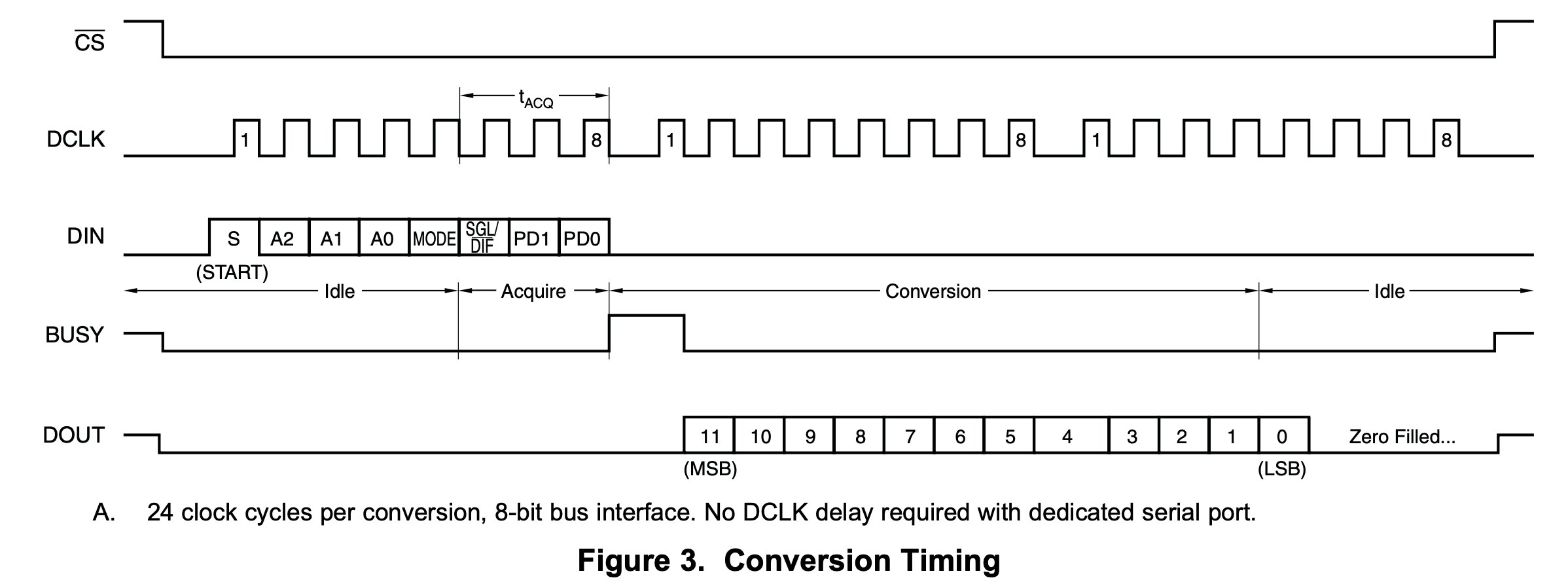
Secondly, the current behavior of my application can be explained through the Timing Diagram as follow.
Per the diagram, the BUSY and DOUT go low as soon as the CS goes low. My DOUT and BUSY is currently stay low all the time.
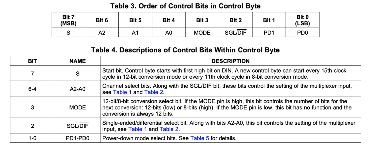
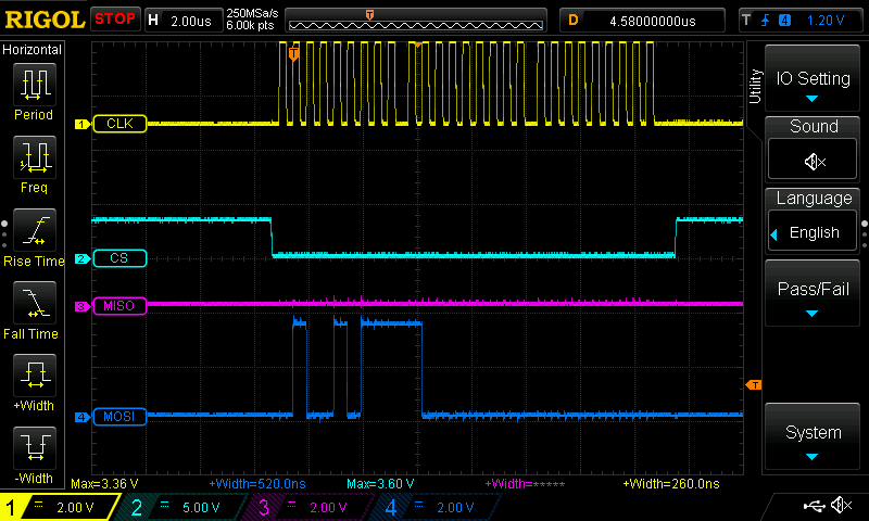
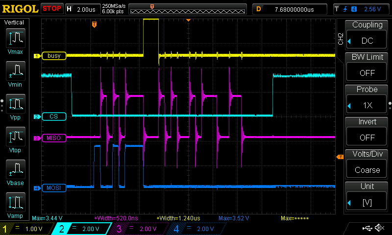
This is the screen shot of the scope with the Control Byte = 0x97 and the subsequent two bytes 0x00 and 0x00 to generate the clock for the DOUT to send in the data.
Here is the message frame.
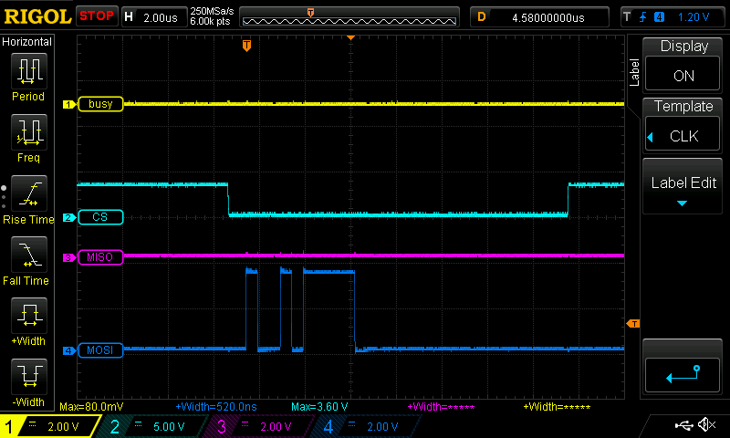
And now is the same message frame but with the BUSY line.
Below is my code
/*
 * src_ads8741.c
 *
 *
 *      The device is using SSI2 of TM4C1294 Pin assignment is as follow:
 *      SPI MOSI - PQ2 - SSI3XDATA0
 *      SPI MISO - PQ3 - SSI3XDATA1
 *      SPI SCL  - PQ0 - SSI3SLCK
 *      SPI ~CS  - PM7 - CHIP SELECT
 *      ADS BUSY - PP3 - BUSY PIN
 */


#include "src_ads8741q1/src_ads8741q1.h"
#include "src_mk_led/mk_led_control.h"

uint32_t pui32DataRx[16];

void init_ads7841q1(uint32_t sysClock) {

    MAP_SysCtlPeripheralEnable(SYSCTL_PERIPH_SSI3);
    MAP_SysCtlPeripheralEnable(SYSCTL_PERIPH_GPIOQ);
    MAP_SysCtlPeripheralEnable(SYSCTL_PERIPH_GPIOM);
    MAP_SysCtlPeripheralEnable(SYSCTL_PERIPH_GPIOP);

    //  Configure SSI3 pins
    MAP_GPIOPinConfigure(GPIO_PQ0_SSI3CLK);
    MAP_GPIOPinConfigure(GPIO_PQ2_SSI3XDAT0);   //MISO
    MAP_GPIOPinConfigure(GPIO_PQ3_SSI3XDAT1);   //MOSI
    MAP_GPIOPinTypeSSI(GPIO_PORTQ_BASE, GPIO_PIN_0 | GPIO_PIN_2 | GPIO_PIN_3);

    //  Setup SPI: 2MHz, 8 bit data, mode 0
    MAP_SSIClockSourceSet(SSI3_BASE, SSI_CLOCK_SYSTEM);
    MAP_SSIConfigSetExpClk(SSI3_BASE, sysClock, SSI_FRF_MOTO_MODE_0,
                           SSI_MODE_MASTER, 2000000, 24);
//    MAP_SSIAdvModeSet(SSI3_BASE, SSI_ADV_MODE_LEGACY);
    MAP_SSIEnable(SSI3_BASE);

    //  Empty receiving buffer
    uint32_t dummy[1];
    while (MAP_SSIDataGetNonBlocking(SSI3_BASE, &dummy[0]));

    //  Configure chip select pin
    MAP_GPIOPinTypeGPIOOutput(GPIO_PORTM_BASE, GPIO_PIN_7);
    ads7841q1_chip_select(UNSELECT);
    // Configure BUSY pin
    MAP_GPIOPinTypeGPIOInput(GPIO_PORTP_BASE, GPIO_PIN_3);
}

void ads7841q1_read_data() {
    uint32_t buffer_data[3] = {0, 0, 0};
    MAP_GPIOPinWrite(GPIO_PORTM_BASE, GPIO_PIN_7, 0);

    /* Send In Control Byte */
    SSIDataPut(SSI3_BASE, 0x97);
    SSIDataGet(SSI3_BASE, &buffer_data[0]);

    SSIDataPut(SSI3_BASE, 0x00);
    SSIDataGet(SSI3_BASE, &buffer_data[1]);

    SSIDataPut(SSI3_BASE, 0x00);
    SSIDataGet(SSI3_BASE, &buffer_data[2]);
    while(SSIBusy(SSI3_BASE)){}


    MAP_GPIOPinWrite(GPIO_PORTM_BASE, GPIO_PIN_7, GPIO_PIN_7);

}

void ads7841q1_chip_select(CHIP_SELECT option) {
    if (option == SELECT) {
        MAP_GPIOPinWrite(GPIO_PORTM_BASE, GPIO_PIN_7, 0);
        set_board_led(BOARD_LED_1, LED_ON);
    } else if (option == UNSELECT) {
        MAP_GPIOPinWrite(GPIO_PORTM_BASE, GPIO_PIN_7, GPIO_PIN_7);
        set_board_led(BOARD_LED_1, LED_OFF);
    }
}

void ads7841q1_check_busy() {
    if(GPIOPinRead(GPIO_PORTP_BASE, GPIO_PIN_3) == GPIO_PIN_3) {
        set_board_led(BOARD_LED_2, LED_ON);
    } else {
        set_board_led(BOARD_LED_2, LED_OFF);
    }
}
I've try different mode .i.e SSI_FRF_MOTO_MODE_0 through SSI_FRF_MOTO_MODE_3
In the main.c the I initialize the function init_ads7841q1() before the while loop and put the ads7841q1_read_data() inside the while loop to generate the communication.
The strange things is that the application works just find when using the GUI application come with the booster pack but doesn't work with my application. I don't know what I miss and I am desperate...
I really appreciate the help from you guys.
Let me know if you need me to provide with more information.
Thanks,
Alex


