This thread has been locked.

If you have a related question, please click the "Ask a related question" button in the top right corner. The newly created question will be automatically linked to this question.

EK-TM4C1294XL: External GPIO pull downs on PWM pins

Guru 54087 points
Part Number: EK-TM4C1294XL
Other Parts Discussed in Thread: TIDA-00778, LM3S8971, UCC27714, LM94022, , TMS320F28027

Hello group,

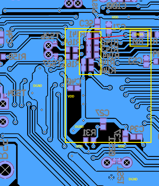
I have been pondering ramifications ADC SNR by 20K pull downs near the MCU pins tied to digital ground, 6 PWM outputs. The PWM output traces lead to analog driver 100k internal pull downs 2" away. The parallel resistances 20K reduces 100k internal input pull downs to roughly 16k overall. Seemingly this practice of adding 10-20k pull downs to analog gate drivers is a breading ground for high frequency PWM riding on ground. 

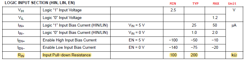
How does that impact SNR of ADC samples and stability? It seems TI engineers TIDA-00778 added 10K pull downs likely for reason POR pin float, any guesses? Typically gate drivers have 100-200k internal pull downs on the inputs so why add any parallel resistance and dampen GPIO current slew? Has there been any study by TI to show how PWM signal injection to MCU ground can or will lead to ADC issues?

Roughly 167µV of current dumped to digital ground x 6 GPIO pins or 1.002mA every 50µs at 20Khz. Do GPIO pins glitch during POR or change state if low impedance resistance is not placed directly near the MCU package pins?

Perhaps one plausible reason for adding any parallel resistor pull downs was to lower the trace impedance if GPIO glitching should randomly occur? This same practice of adding 20k pull downs to GPIO was present on the LM3S8971 motor RDK but only on the low side near the gate driver input also having internal 400k pull downs.

  • You are correct. The usual reason for adding pull down resistors to the PWM outputs is to keep those pins in a low state when the device is in reset. At that time the pins are in high-impedance state and could float high if no pull down is used.

    Even with an equivalent 16K Ohm pull down resistance, the switching PWM signal is not likely to affect the ADC, particularly if proper attention was made digital and analog grounds. It is more likely that the load switched by the PWM will affect the ADC.

  • Hello Bob,

    Bob Crosby said:
    The usual reason for adding pull down resistors to the PWM outputs is to keep those pins in a low state when the device is in reset.

    The question left unanswered why add lower value pull downs when the analog device such as UCC27714 has much greater value pull downs already? Seemingly the device engineers had similar questions as to how to avoid PWM on the ground plane. They obviously designed the pull down values 100k - 400k for some reason, my guess was to avoid power supply ripple from current loading VDD rail.

    Bob Crosby said:
    Even with an equivalent 16K Ohm pull down resistance, the switching PWM signal is not likely to affect the ADC

    The 6 pull downs are located directly under the MCU (R141-R146) and tie to the DGND rail pin that have dedicated single VIA to top side GND pins. My concern is direct feed back of PWM into the MCU on the same rail as AGND ties to via R0 isolation. It seems there is far to much LSB rolling digital 10ths place on all decimal values even with extensive SW filtering. R1 is now DNP but makes the rolling value issue worse when tied to AGND plane and R0 was made DNP.   

    And there is direct trace (red line) to R0 for AGND ties to DGND VIA of 6 PWM pull downs. I was afraid to remove the 6x 20k pull downs but think I'm being silly when 600V analog driver was designed with 100-400k pull downs. Would it not be prudent to remove the 6x 20k pull downs for ADC to have more stable AGND? Again I'm confused seeing TI engineers add 10k pull downs for the same gate driver (UCC27714) and no explanation as to why they done did that. Seemingly they had not used the parallel resistance formula that 400k/10k is even less pull down on the GPIO ports. I have the slew rate set to 8mA for the PWM ports but question current loading VDD rail without good reason.

  • Bob Crosby said:
    It is more likely that the load switched by the PWM will affect the ADC.

    I partially agree but don't see much sample change after x6 drives PWM are running, only on start up as described below. Also occurs to me (now) there are two battle fronts around PWM drive. ADC sample SNR with x6 PWM riding on digital ground, seemingly should be avoided around the MCU ground plane. Simply can not set ADC0 for x16 oversampling (described below) as it will effect FOC motion control and phase current readings in a very bad way. 

    Oddly decimal digit roaming also occurs in the 100's,10's,1's place in 100 5ms intervals of DC bus voltage IE sample counts, even when x6 PWM pins are disabled. Only GPTM0 CCP0 25Khz box fan speed control is always enabled and 4 leads to fan have multiple ferrite beads for cleaner taco edge counts. In order to get temperature readings stable of two LM94022, ADC1 required 64x over sample, TSN 0x6 encoding, trigger processor 1 second intervals with x6 PWM enabled.

    It seems ADC0 has very unstable sample points via IE and random cyclic roaming in 100's, 10s, 1's, 10ths decimal place holder. Increasing capacitance of analog divider is detrimental, anything >50pF allow voltage transient to club MCU into BOR, even with 3v3 TVS placed on divider. So x6 PWM pull downs may be adding to an existing problem as counts had similar decimal roaming on EK-TM4C1294XL launch pad. I had become immune (ignored) the ADC counts issue over the years, even the LM3S8971 ADC did the same thing.

  • Since your questions are around the design of the TIDA-00778, which uses a TMS320F28027 processor, I will transfer this thread to that group.

  • Yet problem reported revolves around  EK-TM4C1294 MCU and being used with yet another vendors analog gate driver. The TIDA-00778 and UCC27714 were merely examples of how the industry and other MCU manufactures were/have put similar pull downs on PWM GPIO pins. The question was why would the 1294 MCU need to have secondary 10k-20k pull down counter measures on the GPIO pins.

    ADC0 samples seem to get more random as PWM drive is enabled, perhaps that is typical ADC behavior without oversampling enabled? Some of this random digit hunting seems to occur result of the serial output speed of the variable/s and reporting peripherals. For instance at 100MBPS (EMAC0) the bus voltage variable 1's,10ths place are fairly stable at all times for DC bus voltage. Yet same variable output via  GPTM6 (5ms) x10 or 50ms intervals via UART0 to an LCD display, 1's and 10ths places are rolling digits often even 100's place can be seen toggling by count of ±1. This toggling is mostly noticed on DC bus volts where watts/Amps are highly periodic and expected so. 

  • I took the time to post the PCB layout and show the 20k resistor placements proximity to AGND and you think this another MCU besides EK-TM4C1294?

  • Posted this side question to aid in the discovery of answers for TM4C1294 thread.

    https://e2e.ti.com/support/power-management/f/196/t/931197

  • That is probably the right place to post your question. It looks to me like the additional pull-down was added because the internal 400K Ohm pull-down resistor on the UCC27714 is not sufficient to handle the maximum leakage out of the input pin (5uA)  and still guarantee a low (below 1.2V). Granted, 10K may be excessive, but I still suspect it causes no issues. Replace the 10K with 100K, it will still provide a pull-down strength that will keep the worst case leakage from causing more than 1V on the input pin while the micro is in reset. I predict it will not change your A to D performance.

  • The actual analog driver pull downs are 100K Min 200k Max. Agree it seems safe to remove 20k pull downs and keep slew rate GPIO (8mA) sink/source. The 5uA leakage is something I never considered and pondered to update 100k but parallel again divides to 50k. Seemingly better to stop inverter dv/dt entry point to GNDA of the ADC simply remove the source point. That hidden inverter dv/dt causes havoc yet luck has it DGND is much quieter than AGND and they are separated on the bottom side foil. The 3 SMP buck regulators diodes dump to AGND on the other side of 0R where AGND becomes DGND, amazed it works fairly well to isolate MCU from AGND noise. 

    The actual analog driver pull downs sink/source via internal resistors shown VIN +5v. Also 51R filter in series with each GPIO drive placed near the analog IC inputs should keep 5uA leakage from entering gate driver. For some odd reason the UCC27714 kept shorting out the center driver HO output.


  • Hi Bob,

    DMM indicated 15.9k before removing 20k's and GPIO pins returned to 111.7k, the lower end of device specification. Noted in electrical specifications TM4C shows 60µA InJ DC injection current is roughly 30µA via 111.7k pull downs at the analog driver by ohms law. The 15.9k that could exceeded 60µA specification (210µV) though inverter DC ramps with  VDD and has 330 ohm 10 watt series bypass contactor. Seemingly Dc injection current is a good reason to not put low value pull downs on GPIO in parallel with analog gate driver pull downs. There was no rise on GPIO pins during POR after removal indicates 100k was suffice. 

    I do notice minor ADC improvement being less rotation speed in random counts with PWM enabled but still not entirely stable. There is obviously other sources inflicting these counts during idle time too. The LCD post code only updates DC bus voltage when a change occurs in the variable/s otherwise it skips the update transmit. That is how all the LCD variable updates occur as not to overwhelm UART with redundant data. Remain confused how EMAC0 seems to ignore ±1 count changes in the 10's position when the LCD is ±2 or 3 counts.

    Thanks for having a look at this ;-)