This thread has been locked.

If you have a related question, please click the "Ask a related question" button in the top right corner. The newly created question will be automatically linked to this question.

TMS320F280049: F280049 SDFM data acquisition issue

Part Number: TMS320F280049
Other Parts Discussed in Thread: AMC1306EVM

Hi

I use sdfm_ex5_filter_sync_fifo_cpuread example to check data acquisition from AMC1306EVM board.

I made the following changes to the code:

1. Use PWM1 to provide SDFM an 10MHz clock(for both AMC1306EVM and SD1.C1).

2. Use DACA to provide a 0 - 0.5V sawtooth output to AMC1306EVM. (Use internal +1.65V as voltage reference)

    DAC data change is done at ISR sdfmFIFO1ISR after data has been converted. (I have confirmed DACA output)

3. To check if the data is correct, the program saves PWM8.TBCTR and 3 converted data from FIFO, so

    I can check if data acquisition time is correct (it can also as a delimiter to distinguish which 3 data are got at the same time).

4. Only check SDFM1.Filter1  and set SDFM1.D1 to GPIO16, SDFM1.C1 to GPIO17.

The changed code is as follows:

//###########################################################################
//
// FILE:   sdfm_ex5_filter_sync_fifo_cpuread.c
//
// TITLE:  SDFM Type 1 Filter FIFO Example.
//
//! \addtogroup driver_example_list
//! <h1> SDFM Type 1 Filter FIFO </h1>
//!
//! This example configures SDFM1 filter to demonstrate data read through
//! CPU in FIFO & non-FIFO mode. Data filter is configured in mode 0
//! to select SINC3 filter with OSR of 256. Filter output is configured
//! for 16-bit format and data shift of 10 is used.
//!
//! This example demonstrates the FIFO usage if enabled. FIFO length is set
//! at 16 and data ready interrupt is configured to be triggered when FIFO is
//! full. In this example, SDFM filter data is read by CPU in SDFM Data Ready
//! ISR routine.
//!
//! \b External \b Connections \n
//!    Connect Sigma-Delta streams to (SD-D1, SD-C1 to SD-D4,SD-C4)
//!    on GPIO24-GPIO31
//!
//! \b Watch \b Variables \n
//! -  \b filter1Result - Output of filter 1
//!
//
//###########################################################################
// $TI Release: F28004x Support Library v1.09.00.00 $
// $Release Date: Thu Mar 19 07:26:52 IST 2020 $
// $Copyright:
// Copyright (C) 2020 Texas Instruments Incorporated - http://www.ti.com/
//
// Redistribution and use in source and binary forms, with or without 
// modification, are permitted provided that the following conditions 
// are met:
// 
//   Redistributions of source code must retain the above copyright 
//   notice, this list of conditions and the following disclaimer.
// 
//   Redistributions in binary form must reproduce the above copyright
//   notice, this list of conditions and the following disclaimer in the 
//   documentation and/or other materials provided with the   
//   distribution.
// 
//   Neither the name of Texas Instruments Incorporated nor the names of
//   its contributors may be used to endorse or promote products derived
//   from this software without specific prior written permission.
// 
// THIS SOFTWARE IS PROVIDED BY THE COPYRIGHT HOLDERS AND CONTRIBUTORS 
// "AS IS" AND ANY EXPRESS OR IMPLIED WARRANTIES, INCLUDING, BUT NOT 
// LIMITED TO, THE IMPLIED WARRANTIES OF MERCHANTABILITY AND FITNESS FOR
// A PARTICULAR PURPOSE ARE DISCLAIMED. IN NO EVENT SHALL THE COPYRIGHT 
// OWNER OR CONTRIBUTORS BE LIABLE FOR ANY DIRECT, INDIRECT, INCIDENTAL, 
// SPECIAL, EXEMPLARY, OR CONSEQUENTIAL DAMAGES (INCLUDING, BUT NOT 
// LIMITED TO, PROCUREMENT OF SUBSTITUTE GOODS OR SERVICES; LOSS OF USE,
// DATA, OR PROFITS; OR BUSINESS INTERRUPTION) HOWEVER CAUSED AND ON ANY
// THEORY OF LIABILITY, WHETHER IN CONTRACT, STRICT LIABILITY, OR TORT 
// (INCLUDING NEGLIGENCE OR OTHERWISE) ARISING IN ANY WAY OUT OF THE USE 
// OF THIS SOFTWARE, EVEN IF ADVISED OF THE POSSIBILITY OF SUCH DAMAGE.
// $
//###########################################################################

//
// Included Files
//
#include "driverlib.h"
#include "device.h"
#include <stdio.h>

#define JIAKAI
//
// Defines
//
#define MAX_SAMPLES               1024
#define FIFO_INT_NUM              3U
#define SDFM_FILTER_ENABLE 0x2U

//
// Macro to enable FIFO mode. Make it zero to disable
// FIFO mode.
//
#define ENABLE_FIFO               1

//
// Globals
//
int16_t  filter1Result[200];
#pragma DATA_SECTION(filter1Result, "Filter1_RegsFile");

//
// Function Prototypes
//
void configureSDFMPins(void);
void initEPWM(uint32_t epwmInstance);
void configureDAC(void);
//
// ISRs
//
__interrupt void sdfmFIFO1ISR(void);
__interrupt void sdfm1ErrorISR(void);

//
// Main
//
void main(void)
{
    //
    // Initialize device clock and peripherals
    //
    Device_init();

    //
    // Setup GPIO by disabling pin locks and enabling pullups
    //
    Device_initGPIO();

    //
    // Initialize PIE and clear PIE registers. Disables CPU interrupts.
    //
    Interrupt_initModule();

    //
    // Initialize the PIE vector table with pointers to the shell Interrupt
    // Service Routines (ISR).
    //
    Interrupt_initVectorTable();

    //
    // Interrupts that are used in this example are re-mapped to
    // ISR functions found within this file.
    //
    Interrupt_clearACKGroup(INTERRUPT_ACK_GROUP5);
    Interrupt_register(INT_SDFM1DR1, sdfmFIFO1ISR);
    Interrupt_register(INT_SDFM1, sdfm1ErrorISR);

    //
    // Enable SDFM1 interrupts(Data Ready & Error interrupts)
    //
#if (0) // need to move to the palce that all devices are initialized
    Interrupt_enableMaster();
    Interrupt_enable(INT_SDFM1DR1);
    Interrupt_enable(INT_SDFM1);
#endif
    initEPWM(EPWM8_BASE);

    //
    // Configure GPIO pins as SDFM pins
    //
    configureSDFMPins();

    //
    // Input Control Unit
    //
    // Configure Input Control Unit: Modulator Clock rate = Modulator data rate
    //
    SDFM_setupModulatorClock(SDFM1_BASE, SDFM_FILTER_1,
                             SDFM_MODULATOR_CLK_EQUAL_DATA_RATE);

    //
    // Data Filter Unit
    //

    // Configure Data Filter Unit - filter type, OSR value and
    // enable / disable data filter
    //
    SDFM_configDataFilter(SDFM1_BASE, (SDFM_FILTER_1 | SDFM_FILTER_SINC_3 |
           SDFM_SET_OSR(256)), (SDFM_DATA_FORMAT_16_BIT | SDFM_FILTER_ENABLE |
           SDFM_SHIFT_VALUE(0x000A)));

#if (ENABLE_FIFO)
        //
        // Set data ready interrupt source as fifo interrupt
        //
        SDFM_setDataReadyInterruptSource(SDFM1_BASE, SDFM_FILTER_1,
                                         SDFM_DATA_READY_SOURCE_FIFO);

        //
        // Enable FIFO and set the FIFO interrupt level
        //
        SDFM_enableFIFOBuffer(SDFM1_BASE, SDFM_FILTER_1);

        SDFM_setFIFOInterruptLevel(SDFM1_BASE, SDFM_FILTER_1, FIFO_INT_NUM);

        SDFM_enableInterrupt(SDFM1_BASE, SDFM_FILTER_1,
                         (SDFM_FIFO_INTERRUPT | SDFM_FIFO_OVERFLOW_INTERRUPT));
#else
        //
        // Set data ready interrupt source as fifo interrupt
        //
        SDFM_setDataReadyInterruptSource(SDFM1_BASE, SDFM_FILTER_1,
                                         SDFM_DATA_READY_SOURCE_DIRECT);

        SDFM_enableInterrupt(SDFM1_BASE, SDFM_FILTER_1,
                             SDFM_DATA_FILTER_ACKNOWLEDGE_INTERRUPT);
#endif


    //
    // Enable Master filter bit: Unless this bit is set none of the filter
    // modules can be enabled. All the filter modules are synchronized when
    // master filter bit is enabled after individual filter modules are enabled.
    //
    SDFM_enableMasterFilter(SDFM1_BASE);

    //
    // Use PWM8.CMPA signals to synchronize the filters.
    //
#if (0)
    SDFM_disableExternalReset(SDFM1_BASE, SDFM_FILTER_1);
#else
    SDFM_enableExternalReset(SDFM1_BASE, SDFM_FILTER_1);
    SDFM_setPWMSyncSource(SDFM1_BASE, SDFM_FILTER_1, SDFM_SYNC_PWM8_SOCA);
    SDFM_enableWaitForSync(SDFM1_BASE, SDFM_FILTER_1);
#endif

    //
    // Enable modulator failure interrupt, disable threshold interrupts
    //
    SDFM_enableInterrupt(SDFM1_BASE, SDFM_FILTER_1,
                         SDFM_MODULATOR_FAILURE_INTERRUPT);

    SDFM_disableInterrupt(SDFM1_BASE, SDFM_FILTER_1,
                          (SDFM_HIGH_LEVEL_THRESHOLD_INTERRUPT |
                           SDFM_LOW_LEVEL_THRESHOLD_INTERRUPT));

    configureDAC();

    while((HWREGH(EPWM8_BASE + EPWM_O_TBCTR)) < 550);

    //
    // Enable master interrupt so that any of the filter interrupts can trigger
    // by SDFM interrupt to CPU
    //
    SDFM_enableMasterInterrupt(SDFM1_BASE);

#if (1) // need to move to the palce that all devices are initialized
    Interrupt_enableMaster();
    Interrupt_enable(INT_SDFM1DR1);
    Interrupt_enable(INT_SDFM1);
#endif

    //
    // Enable Global Interrupt (INTM) and realtime interrupt (DBGM)
    //
    EINT;
    ERTM;

    //
    // Wait for an interrupt
    //
    while(1);
}

//
// sdfm1ErrorISR - SDFM1 Error ISR
//
unsigned long cntErr = 0;
__interrupt void sdfm1ErrorISR(void)
{
    //
    // Clear SDFM flag register (SDIFLG)
    //
    SDFM_clearInterruptFlag(SDFM1_BASE, SDFM_MASTER_INTERRUPT_FLAG |
                            0xFFFF);
    cntErr++;

    //
    // Acknowledge this interrupt to receive more interrupts from group 5
    //
    Interrupt_clearACKGroup(INTERRUPT_ACK_GROUP5);
}

#define PWM_TBCTR(_p)       *((uint16_t *)(0x3F04 + 0x100 * (_p)))
unsigned long cntDat = 0;

//
// sdfmFIFO1ISR - SDFM FIFO1 ISR
//
__interrupt void sdfmFIFO1ISR(void)
{
    uint16_t i;
    static uint16_t loopCounter1 = 0;

#if (0)
    SDFM_setOutputDataFormat(SDFM1_BASE, SDFM_FILTER_1,
                             SDFM_DATA_FORMAT_16_BIT);
#endif

    cntDat++;
    //
    // Read SDFM flag register (SDIFLG)
    //
//    if(loopCounter1 >= MAX_SAMPLES)
//    {
//        loopCounter1 = 0;
//        ESTOP0;
//    }

    if(SDFM_getFIFOISRStatus(SDFM1_BASE, SDFM_FILTER_1) == 0x1U)
    {
        filter1Result[loopCounter1] = PWM_TBCTR(8); if (++loopCounter1 >= 200) loopCounter1 = 0;
        for(i = 0; i < FIFO_INT_NUM; i++)
        {
            filter1Result[loopCounter1] =
                         (int16_t)(SDFM_getFIFOData(SDFM1_BASE,
                                                    SDFM_FILTER_1) >> 16U);
            if (++loopCounter1 >= 200) loopCounter1 = 0;
        }

    }
    else if(SDFM_getNewFilterDataStatus(SDFM1_BASE, SDFM_FILTER_1) == 0x1U)
    {
        filter1Result[loopCounter1++] =
               (int16_t)(SDFM_getFilterData(SDFM1_BASE, SDFM_FILTER_1) >> 16U);
        if (++loopCounter1 >= 200) loopCounter1 = 0;
    }

    {
        static int dacVal = 0, iDelta = 5;
        dacVal += iDelta; if (dacVal >= 500) dacVal = 0;

        DAC_setShadowValue(DACA_BASE, (int)(dacVal * 3300.0 / 4095.0));
    }

    //
    // Clear SDFM flag register (SDIFLG)
    //
    SDFM_clearInterruptFlag(SDFM1_BASE, SDFM_MASTER_INTERRUPT_FLAG |
                            SDFM_FILTER_1_FIFO_INTERRUPT_FLAG      |
                            SDFM_FILTER_1_NEW_DATA_FLAG            |
                            SDFM_FILTER_1_FIFO_OVERFLOW_FLAG);

    //
    // Acknowledge this interrupt to receive more interrupts from group 5
    //
    Interrupt_clearACKGroup(INTERRUPT_ACK_GROUP5);
}

//
// configureSDFMPins - Configure SDFM GPIOs
//
void configureSDFMPins(void)
{
    uint16_t pin;
#ifdef JIAKAI
    for(pin = 16; pin <= 17; pin++)
    {
//        GPIO_setDirectionMode(pin, GPIO_DIR_MODE_IN);
        GPIO_setMasterCore(pin, GPIO_CORE_CPU1);
        GPIO_setPadConfig(pin, GPIO_PIN_TYPE_STD);
        GPIO_setQualificationMode(pin, GPIO_QUAL_ASYNC);
    }
    GPIO_setPinConfig(GPIO_16_SD1_D1);
    GPIO_setPinConfig(GPIO_17_SD1_C1);
#else
    for(pin = 24; pin <= 31; pin++)
    {
        GPIO_setDirectionMode(pin, GPIO_DIR_MODE_IN);
        GPIO_setMasterCore(pin, GPIO_CORE_CPU1);
        GPIO_setPadConfig(pin, GPIO_PIN_TYPE_STD);
        GPIO_setQualificationMode(pin, GPIO_QUAL_ASYNC);
    }

    //
    // Configure GPIO16-GPIO31 as SDFM pins
    //
    GPIO_setPinConfig(GPIO_24_SD_D1);
    GPIO_setPinConfig(GPIO_25_SD_C1);
    GPIO_setPinConfig(GPIO_26_SD_D2);
    GPIO_setPinConfig(GPIO_27_SD_C2);
    GPIO_setPinConfig(GPIO_28_SD_D3);
    GPIO_setPinConfig(GPIO_29_SD_C3);
    GPIO_setPinConfig(GPIO_30_SD_D4);
    GPIO_setPinConfig(GPIO_31_SD_C4);
#endif
}


//
// Configure DAC - Setup the reference voltage and output value for the DAC
//
void configureDAC(void)
{
    //
    // Set internal +1.65v as the DAC reference voltage.
    // Edit here to use ADC VREF as the reference voltage.
    //
    ADC_setVREF(ADCA_BASE, ADC_REFERENCE_INTERNAL, ADC_REFERENCE_3_3V);
    DAC_setReferenceVoltage(DACA_BASE, DAC_REF_ADC_VREFHI); // DAC_REF_VDAC
    DAC_setGainMode(DACA_BASE, DAC_GAIN_TWO);

    //
    // Enable the DAC output
    //
    DAC_enableOutput(DACA_BASE);

    //
    // Set the DAC shadow output to 0
    //
    DAC_setShadowValue(DACA_BASE, 0);

    //
    // Delay for buffered DAC to power up
    //
    DEVICE_DELAY_US(10);
}

//
// initEPWM - Initialize specified EPWM settings
//
void initEPWM(uint32_t epwmInstance)
{
    //
    // Disable sync(Freeze clock to PWM as well)
    //
    SysCtl_disablePeripheral(SYSCTL_PERIPH_CLK_TBCLKSYNC);
    EPWM_disableADCTrigger(epwmInstance, EPWM_SOC_A);

    //
    // Setup TBCLK: Configure timer period = 801 TBCLKs, phase = 0 &
    // clear counter
    //
    EPWM_setTimeBasePeriod(epwmInstance, 0xFFF0);
    EPWM_setPhaseShift(epwmInstance, 0U);
    EPWM_setTimeBaseCounter(epwmInstance, 0U);

    //
    // Set CMPA value
    //
    EPWM_setCounterCompareValue(epwmInstance, EPWM_COUNTER_COMPARE_A, 200U);

    //
    // Setup counter mode
    //
    EPWM_setTimeBaseCounterMode(epwmInstance, EPWM_COUNTER_MODE_UP);
    EPWM_setClockPrescaler(epwmInstance,
                           EPWM_CLOCK_DIVIDER_1,
                           EPWM_HSCLOCK_DIVIDER_1);

    //
    // Set actions:
    // Toggle PWMxA on event A, up-count
    // Toggle PWMxB on event A, up-count
    //
    GPIO_setPadConfig(0, GPIO_PIN_TYPE_STD);
    GPIO_setPinConfig(GPIO_0_EPWM1_A);
    GPIO_setPadConfig(1, GPIO_PIN_TYPE_STD);
    GPIO_setPinConfig(GPIO_1_EPWM1_B);
    EPWM_setTimeBasePeriod(EPWM1_BASE, 4);     // PWM1 period: 0.1us
    EPWM_setTimeBaseCounterMode(EPWM1_BASE, EPWM_COUNTER_MODE_UP);
    EPWM_setClockPrescaler(EPWM1_BASE,
                           EPWM_CLOCK_DIVIDER_1,
                           EPWM_HSCLOCK_DIVIDER_1);
    EPWM_setActionQualifierAction(EPWM1_BASE,
                                  EPWM_AQ_OUTPUT_A,
                                  EPWM_AQ_OUTPUT_TOGGLE,
                                  EPWM_AQ_OUTPUT_ON_TIMEBASE_PERIOD);
//                                EPWM_AQ_OUTPUT_ON_TIMEBASE_UP_CMPA);
    EPWM_setActionQualifierAction(EPWM1_BASE,
                                  EPWM_AQ_OUTPUT_B,
                                  EPWM_AQ_OUTPUT_TOGGLE,
                                  EPWM_AQ_OUTPUT_ON_TIMEBASE_PERIOD);
//                                EPWM_AQ_OUTPUT_ON_TIMEBASE_UP_CMPB);

//#ifndef JIAKAI
    //
    // Configure SOCA signal
    //
    //
    EPWM_setADCTriggerSource(epwmInstance, EPWM_SOC_A, EPWM_SOC_TBCTR_U_CMPA);
    EPWM_setADCTriggerEventPrescale(epwmInstance, EPWM_SOC_A, 1);
    EPWM_enableADCTrigger(epwmInstance, EPWM_SOC_A);
//#endif

    //
    // Enable sync and clock to PWM
    //
    SysCtl_enablePeripheral(SYSCTL_PERIPH_CLK_TBCLKSYNC);
}

//
// End of file
//

After running the code, I found the ISR is entered at an accurate time but 3 acquisition data are not even close to each other (see below).

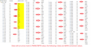
Looking forward a TI technician or expert to point out the issue in the program.

Thanks,

Jiakai

  • Jiakai,

    In your code, PWM8 is configured to generate sync pulse to SDFM every 655.2 us. So, SDFM.FILTER1 (data filter) will get reset every 655.2 us. Once a Sinc3 filter is reset, 1st two samples will be incorrect and filter produces correct filter output only from 3rd sample. That is the reason why you are seeing two incorrect samples. To avoid this problem ignore first 2 samples and start recording from 3rd sample.

    Another suggestion would be to first provide DC input rather than saw tooth input to debug this problem.

    Regards,

    Manoj

  • Hi Manoj,

    Awesome!

    You are right! I have confirmed it.

    Thank you very much!

    Jiakai

  • Hi Manoj,

    I have tried to calculate SDFM results from registry value to voltage value as below (AMC1306EVM input comes from DACA

    and DACA output signal is a sawtooth waveform from 0 to 0.25v):

    buf[loopCounter1] = 0.25 * (SDFM_getFIFOData(SDFM1_BASE, SDFM_FILTER_1) >> 16U) / ((1L*256*256*256) >> 10);

    In above statement, 0.25 is Vclipping value (250mv).

    The voltage values are saved to buf array (I merge RAMLS6 and RAMLS7 to RAMLS5 in 28004x_sdfm_ram_Lnk.cmd), 

    the array values are displayed as follows:

    From the above graph, the maximum value is near to 0.125v (only 1/2 of the real input value).

    Do I have any mistake on the calculation? What's the correct calculation method?

    The source code is as follows:

    //###########################################################################
    //
    // FILE:   sdfm_ex5_filter_sync_fifo_cpuread.c
    //
    // TITLE:  SDFM Type 1 Filter FIFO Example.
    //
    //! \addtogroup driver_example_list
    //! <h1> SDFM Type 1 Filter FIFO </h1>
    //!
    //! This example configures SDFM1 filter to demonstrate data read through
    //! CPU in FIFO & non-FIFO mode. Data filter is configured in mode 0
    //! to select SINC3 filter with OSR of 256. Filter output is configured
    //! for 16-bit format and data shift of 10 is used.
    //!
    //! This example demonstrates the FIFO usage if enabled. FIFO length is set
    //! at 16 and data ready interrupt is configured to be triggered when FIFO is
    //! full. In this example, SDFM filter data is read by CPU in SDFM Data Ready
    //! ISR routine.
    //!
    //! \b External \b Connections \n
    //!    Connect Sigma-Delta streams to (SD-D1, SD-C1 to SD-D4,SD-C4)
    //!    on GPIO24-GPIO31
    //!
    //! \b Watch \b Variables \n
    //! -  \b filter1Result - Output of filter 1
    //!
    //
    //###########################################################################
    // $TI Release: F28004x Support Library v1.09.00.00 $
    // $Release Date: Thu Mar 19 07:26:52 IST 2020 $
    // $Copyright:
    // Copyright (C) 2020 Texas Instruments Incorporated - http://www.ti.com/
    //
    // Redistribution and use in source and binary forms, with or without 
    // modification, are permitted provided that the following conditions 
    // are met:
    // 
    //   Redistributions of source code must retain the above copyright 
    //   notice, this list of conditions and the following disclaimer.
    // 
    //   Redistributions in binary form must reproduce the above copyright
    //   notice, this list of conditions and the following disclaimer in the 
    //   documentation and/or other materials provided with the   
    //   distribution.
    // 
    //   Neither the name of Texas Instruments Incorporated nor the names of
    //   its contributors may be used to endorse or promote products derived
    //   from this software without specific prior written permission.
    // 
    // THIS SOFTWARE IS PROVIDED BY THE COPYRIGHT HOLDERS AND CONTRIBUTORS 
    // "AS IS" AND ANY EXPRESS OR IMPLIED WARRANTIES, INCLUDING, BUT NOT 
    // LIMITED TO, THE IMPLIED WARRANTIES OF MERCHANTABILITY AND FITNESS FOR
    // A PARTICULAR PURPOSE ARE DISCLAIMED. IN NO EVENT SHALL THE COPYRIGHT 
    // OWNER OR CONTRIBUTORS BE LIABLE FOR ANY DIRECT, INDIRECT, INCIDENTAL, 
    // SPECIAL, EXEMPLARY, OR CONSEQUENTIAL DAMAGES (INCLUDING, BUT NOT 
    // LIMITED TO, PROCUREMENT OF SUBSTITUTE GOODS OR SERVICES; LOSS OF USE,
    // DATA, OR PROFITS; OR BUSINESS INTERRUPTION) HOWEVER CAUSED AND ON ANY
    // THEORY OF LIABILITY, WHETHER IN CONTRACT, STRICT LIABILITY, OR TORT 
    // (INCLUDING NEGLIGENCE OR OTHERWISE) ARISING IN ANY WAY OUT OF THE USE 
    // OF THIS SOFTWARE, EVEN IF ADVISED OF THE POSSIBILITY OF SUCH DAMAGE.
    // $
    //###########################################################################
    
    //
    // Included Files
    //
    #include "driverlib.h"
    #include "device.h"
    #include <stdio.h>
    
    #define JIAKAI
    //
    // Defines
    //
    #define MAX_SAMPLES               1024
    #define FIFO_INT_NUM              7U
    #define SDFM_FILTER_ENABLE 0x2U
    
    //
    // Macro to enable FIFO mode. Make it zero to disable
    // FIFO mode.
    //
    #define ENABLE_FIFO               1
    
    //
    // Globals
    //
    #define BUF_SIZE    1024
    int16_t filter1Result[BUF_SIZE];
    float   buf[BUF_SIZE];
    //#pragma DATA_SECTION(filter1Result, "Filter1_RegsFile");
    
    //
    // Function Prototypes
    //
    void configureSDFMPins(void);
    void initEPWM(uint32_t epwmInstance);
    void configureDAC(void);
    //
    // ISRs
    //
    __interrupt void sdfmFIFO1ISR(void);
    __interrupt void sdfm1ErrorISR(void);
    
    //
    // Main
    //
    void main(void)
    {
        //
        // Initialize device clock and peripherals
        //
        Device_init();
    
        //
        // Setup GPIO by disabling pin locks and enabling pullups
        //
        Device_initGPIO();
    
        //
        // Initialize PIE and clear PIE registers. Disables CPU interrupts.
        //
        Interrupt_initModule();
    
        //
        // Initialize the PIE vector table with pointers to the shell Interrupt
        // Service Routines (ISR).
        //
        Interrupt_initVectorTable();
    
        //
        // Interrupts that are used in this example are re-mapped to
        // ISR functions found within this file.
        //
        Interrupt_clearACKGroup(INTERRUPT_ACK_GROUP5);
        Interrupt_register(INT_SDFM1DR1, sdfmFIFO1ISR);
        Interrupt_register(INT_SDFM1, sdfm1ErrorISR);
    
        //
        // Enable SDFM1 interrupts(Data Ready & Error interrupts)
        //
    #if (0) // need to move to the palce that all devices are initialized
        Interrupt_enableMaster();
        Interrupt_enable(INT_SDFM1DR1);
        Interrupt_enable(INT_SDFM1);
    #endif
        initEPWM(EPWM8_BASE);
    
        //
        // Configure GPIO pins as SDFM pins
        //
        configureSDFMPins();
    
        //
        // Input Control Unit
        //
        // Configure Input Control Unit: Modulator Clock rate = Modulator data rate
        //
        SDFM_setupModulatorClock(SDFM1_BASE, SDFM_FILTER_1,
                                 SDFM_MODULATOR_CLK_EQUAL_DATA_RATE);
    
        //
        // Data Filter Unit
        //
    
        // Configure Data Filter Unit - filter type, OSR value and
        // enable / disable data filter
        //
        SDFM_configDataFilter(SDFM1_BASE, (SDFM_FILTER_1 | SDFM_FILTER_SINC_3 |
               SDFM_SET_OSR(256)), (SDFM_DATA_FORMAT_16_BIT | SDFM_FILTER_ENABLE |
               SDFM_SHIFT_VALUE(0x000A)));
    
    #if (ENABLE_FIFO)
            //
            // Set data ready interrupt source as fifo interrupt
            //
            SDFM_setDataReadyInterruptSource(SDFM1_BASE, SDFM_FILTER_1,
                                             SDFM_DATA_READY_SOURCE_FIFO);
    
            //
            // Enable FIFO and set the FIFO interrupt level
            //
            SDFM_enableFIFOBuffer(SDFM1_BASE, SDFM_FILTER_1);
    
            SDFM_setFIFOInterruptLevel(SDFM1_BASE, SDFM_FILTER_1, FIFO_INT_NUM);
    
            SDFM_enableInterrupt(SDFM1_BASE, SDFM_FILTER_1,
                             (SDFM_FIFO_INTERRUPT | SDFM_FIFO_OVERFLOW_INTERRUPT));
    #else
            //
            // Set data ready interrupt source as fifo interrupt
            //
            SDFM_setDataReadyInterruptSource(SDFM1_BASE, SDFM_FILTER_1,
                                             SDFM_DATA_READY_SOURCE_DIRECT);
    
            SDFM_enableInterrupt(SDFM1_BASE, SDFM_FILTER_1,
                                 SDFM_DATA_FILTER_ACKNOWLEDGE_INTERRUPT);
    #endif
    
    
        //
        // Enable Master filter bit: Unless this bit is set none of the filter
        // modules can be enabled. All the filter modules are synchronized when
        // master filter bit is enabled after individual filter modules are enabled.
        //
        SDFM_enableMasterFilter(SDFM1_BASE);
    
        //
        // Use PWM8.CMPA signals to synchronize the filters.
        //
    #if (0)
        SDFM_disableExternalReset(SDFM1_BASE, SDFM_FILTER_1);
    #else
        SDFM_enableExternalReset(SDFM1_BASE, SDFM_FILTER_1);
        SDFM_setPWMSyncSource(SDFM1_BASE, SDFM_FILTER_1, SDFM_SYNC_PWM8_SOCA);
        SDFM_enableWaitForSync(SDFM1_BASE, SDFM_FILTER_1);
    #endif
    
        //
        // Enable modulator failure interrupt, disable threshold interrupts
        //
        SDFM_enableInterrupt(SDFM1_BASE, SDFM_FILTER_1,
                             SDFM_MODULATOR_FAILURE_INTERRUPT);
    
        SDFM_disableInterrupt(SDFM1_BASE, SDFM_FILTER_1,
                              (SDFM_HIGH_LEVEL_THRESHOLD_INTERRUPT |
                               SDFM_LOW_LEVEL_THRESHOLD_INTERRUPT));
    
        configureDAC();
    
    //    while((HWREGH(EPWM8_BASE + EPWM_O_TBCTR)) < 550);
    
        //
        // Enable master interrupt so that any of the filter interrupts can trigger
        // by SDFM interrupt to CPU
        //
        SDFM_enableMasterInterrupt(SDFM1_BASE);
    
    #if (1) // need to move to the palce that all devices are initialized
        Interrupt_enableMaster();
        Interrupt_enable(INT_SDFM1DR1);
        Interrupt_enable(INT_SDFM1);
    #endif
    
        //
        // Enable Global Interrupt (INTM) and realtime interrupt (DBGM)
        //
        EINT;
        ERTM;
    
        //
        // Wait for an interrupt
        //
        while(1);
    }
    
    //
    // sdfm1ErrorISR - SDFM1 Error ISR
    //
    unsigned long cntErr = 0;
    __interrupt void sdfm1ErrorISR(void)
    {
        //
        // Clear SDFM flag register (SDIFLG)
        //
        SDFM_clearInterruptFlag(SDFM1_BASE, SDFM_MASTER_INTERRUPT_FLAG |
                                0xFFFF);
        cntErr++;
    
        //
        // Acknowledge this interrupt to receive more interrupts from group 5
        //
        Interrupt_clearACKGroup(INTERRUPT_ACK_GROUP5);
    }
    
    #define PWM_TBCTR(_p)       *((uint16_t *)(0x3F04 + 0x100 * (_p)))
    unsigned long cntDat = 0;
    
    //
    // sdfmFIFO1ISR - SDFM FIFO1 ISR
    //
    float aryCoef[7] = {0.0, 0.0, 0.2, 0.2, 0.2, 0.2, 0.2};
    __interrupt void sdfmFIFO1ISR(void)
    {
        uint16_t i;
        static uint16_t loopCounter1 = 0;
    
    #if (0)
        SDFM_setOutputDataFormat(SDFM1_BASE, SDFM_FILTER_1,
                                 SDFM_DATA_FORMAT_16_BIT);
    #endif
    
        cntDat++;
        //
        // Read SDFM flag register (SDIFLG)
        //
        if(loopCounter1 >= MAX_SAMPLES)
        {
            loopCounter1 = 0;
            ESTOP0;
        } else if(SDFM_getFIFOISRStatus(SDFM1_BASE, SDFM_FILTER_1) == 0x1U)
        {
            buf[loopCounter1] = 0.0;
            filter1Result[loopCounter1] = PWM_TBCTR(8); ++loopCounter1;//if (++loopCounter1 >= BUF_SIZE) loopCounter1 = 0;
            for(i = 0; i < FIFO_INT_NUM; i++)
            {
                int16_t iVal = (int16_t)(SDFM_getFIFOData(SDFM1_BASE, SDFM_FILTER_1) >> 16U);
                filter1Result[loopCounter1] = iVal;
                buf[loopCounter1] = 0.25 * iVal / ((1L*256*256*256) >> 10);
                ++loopCounter1; // if (++loopCounter1 >= BUF_SIZE) loopCounter1 = 0;
            }
    
        }
        else if(SDFM_getNewFilterDataStatus(SDFM1_BASE, SDFM_FILTER_1) == 0x1U)
        {
            filter1Result[loopCounter1++] =
                   (int16_t)(SDFM_getFilterData(SDFM1_BASE, SDFM_FILTER_1) >> 16U);
            if (++loopCounter1 >= 200) loopCounter1 = 0;
        }
    
        {
            static int dacVal = 0, iDelta = 5;
            dacVal += iDelta; if (dacVal >= 250) dacVal = 0;
    
            DAC_setShadowValue(DACA_BASE, (int)(dacVal * 3300.0 / 4095.0));
        }
    
        //
        // Clear SDFM flag register (SDIFLG)
        //
        SDFM_clearInterruptFlag(SDFM1_BASE, SDFM_MASTER_INTERRUPT_FLAG |
                                SDFM_FILTER_1_FIFO_INTERRUPT_FLAG      |
                                SDFM_FILTER_1_NEW_DATA_FLAG            |
                                SDFM_FILTER_1_FIFO_OVERFLOW_FLAG);
    
        //
        // Acknowledge this interrupt to receive more interrupts from group 5
        //
        Interrupt_clearACKGroup(INTERRUPT_ACK_GROUP5);
    }
    
    //
    // configureSDFMPins - Configure SDFM GPIOs
    //
    void configureSDFMPins(void)
    {
        uint16_t pin;
    #ifdef JIAKAI
        for(pin = 16; pin <= 17; pin++)
        {
    //        GPIO_setDirectionMode(pin, GPIO_DIR_MODE_IN);
            GPIO_setMasterCore(pin, GPIO_CORE_CPU1);
            GPIO_setPadConfig(pin, GPIO_PIN_TYPE_STD);
            GPIO_setQualificationMode(pin, GPIO_QUAL_ASYNC);
        }
        GPIO_setPinConfig(GPIO_16_SD1_D1);
        GPIO_setPinConfig(GPIO_17_SD1_C1);
    #else
        for(pin = 24; pin <= 31; pin++)
        {
            GPIO_setDirectionMode(pin, GPIO_DIR_MODE_IN);
            GPIO_setMasterCore(pin, GPIO_CORE_CPU1);
            GPIO_setPadConfig(pin, GPIO_PIN_TYPE_STD);
            GPIO_setQualificationMode(pin, GPIO_QUAL_ASYNC);
        }
    
        //
        // Configure GPIO16-GPIO31 as SDFM pins
        //
        GPIO_setPinConfig(GPIO_24_SD_D1);
        GPIO_setPinConfig(GPIO_25_SD_C1);
        GPIO_setPinConfig(GPIO_26_SD_D2);
        GPIO_setPinConfig(GPIO_27_SD_C2);
        GPIO_setPinConfig(GPIO_28_SD_D3);
        GPIO_setPinConfig(GPIO_29_SD_C3);
        GPIO_setPinConfig(GPIO_30_SD_D4);
        GPIO_setPinConfig(GPIO_31_SD_C4);
    #endif
    }
    
    
    //
    // Configure DAC - Setup the reference voltage and output value for the DAC
    //
    void configureDAC(void)
    {
        //
        // Set internal +1.65v as the DAC reference voltage.
        // Edit here to use ADC VREF as the reference voltage.
        //
        ADC_setVREF(ADCA_BASE, ADC_REFERENCE_INTERNAL, ADC_REFERENCE_3_3V);
        DAC_setReferenceVoltage(DACA_BASE, DAC_REF_ADC_VREFHI); // DAC_REF_VDAC
        DAC_setGainMode(DACA_BASE, DAC_GAIN_TWO);
    
        //
        // Enable the DAC output
        //
        DAC_enableOutput(DACA_BASE);
    
        //
        // Set the DAC shadow output to 0
        //
        DAC_setShadowValue(DACA_BASE, 0);
    
        //
        // Delay for buffered DAC to power up
        //
        DEVICE_DELAY_US(10);
    }
    
    //
    // initEPWM - Initialize specified EPWM settings
    //
    void initEPWM(uint32_t epwmInstance)
    {
        //
        // Disable sync(Freeze clock to PWM as well)
        //
        SysCtl_disablePeripheral(SYSCTL_PERIPH_CLK_TBCLKSYNC);
        EPWM_disableADCTrigger(epwmInstance, EPWM_SOC_A);
    
        //
        // Setup TBCLK: Configure timer period = 801 TBCLKs, phase = 0 &
        // clear counter
        //
        EPWM_setTimeBasePeriod(epwmInstance, 0xFFF0);
        EPWM_setPhaseShift(epwmInstance, 0U);
        EPWM_setTimeBaseCounter(epwmInstance, 0U);
    
        //
        // Set CMPA value
        //
        EPWM_setCounterCompareValue(epwmInstance, EPWM_COUNTER_COMPARE_A, 200U);
    
        //
        // Setup counter mode
        //
        EPWM_setTimeBaseCounterMode(epwmInstance, EPWM_COUNTER_MODE_UP);
        EPWM_setClockPrescaler(epwmInstance,
                               EPWM_CLOCK_DIVIDER_1,
                               EPWM_HSCLOCK_DIVIDER_1);
    
        //
        // Set actions:
        // Toggle PWMxA on event A, up-count
        // Toggle PWMxB on event A, up-count
        //
        GPIO_setPadConfig(0, GPIO_PIN_TYPE_STD);
        GPIO_setPinConfig(GPIO_0_EPWM1_A);
        GPIO_setPadConfig(1, GPIO_PIN_TYPE_STD);
        GPIO_setPinConfig(GPIO_1_EPWM1_B);
        EPWM_setTimeBasePeriod(EPWM1_BASE, 4);     // PWM1 period: 0.1us
        EPWM_setTimeBaseCounterMode(EPWM1_BASE, EPWM_COUNTER_MODE_UP);
        EPWM_setClockPrescaler(EPWM1_BASE,
                               EPWM_CLOCK_DIVIDER_1,
                               EPWM_HSCLOCK_DIVIDER_1);
        EPWM_setActionQualifierAction(EPWM1_BASE,
                                      EPWM_AQ_OUTPUT_A,
                                      EPWM_AQ_OUTPUT_TOGGLE,
                                      EPWM_AQ_OUTPUT_ON_TIMEBASE_PERIOD);
    //                                EPWM_AQ_OUTPUT_ON_TIMEBASE_UP_CMPA);
        EPWM_setActionQualifierAction(EPWM1_BASE,
                                      EPWM_AQ_OUTPUT_B,
                                      EPWM_AQ_OUTPUT_TOGGLE,
                                      EPWM_AQ_OUTPUT_ON_TIMEBASE_PERIOD);
    //                                EPWM_AQ_OUTPUT_ON_TIMEBASE_UP_CMPB);
    
    //#ifndef JIAKAI
        //
        // Configure SOCA signal
        //
        //
        EPWM_setADCTriggerSource(epwmInstance, EPWM_SOC_A, EPWM_SOC_TBCTR_U_CMPA);
        EPWM_setADCTriggerEventPrescale(epwmInstance, EPWM_SOC_A, 1);
        EPWM_enableADCTrigger(epwmInstance, EPWM_SOC_A);
    //#endif
    
        //
        // Enable sync and clock to PWM
        //
        SysCtl_enablePeripheral(SYSCTL_PERIPH_CLK_TBCLKSYNC);
    }
    
    //
    // End of file
    //
    

    thanks,

    Jiakai

  • Jiakai,

    The correlation between analog input of the SD-modulator and SDFM digital filter output is captured in "Theoretical SDFM Filter Output" section in F28388D TRM.

    This information also applies to F280049 SDFM and will be updated in the next release of TRM.

    Regards,

    Manoj


  • Hi Manoj,

    Thank you for your reply.

    I have found the bugs in my code ():

    1. In line 325, the expression is wrong, the correct statement is as follows:

             DAC_setShadowValue(DACA_BASE, (int)(dacVal * 4095.0 / 3300.0));

    2. In line 309, Vclipping is set to 0.25 (250mV), it should be 0.32 (320mV as in the manual).

    thanks,

    Jiakai