Other Parts Discussed in Thread: C2000WARE
Hello Champs,
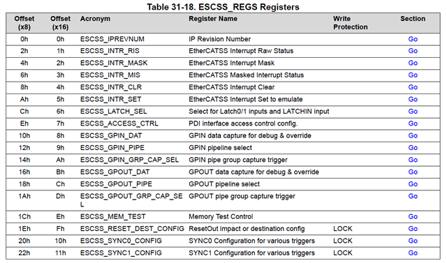
We can only find USB and EtherCAT registers base address for C28 in F2838x TRM but cannot find USB and EtherCAT registers base address for CM.
Would you please help? Thanks!
Best Regards,
Linda