This thread has been locked.

If you have a related question, please click the "Ask a related question" button in the top right corner. The newly created question will be automatically linked to this question.

TMS320F280041: Unable to flash the processor on custom board

Part Number: TMS320F280041
Other Parts Discussed in Thread: TPS5401

Hello,

I have a custom board that uses the TMS320F280041PZ, and right now I am unable to connect to it with the XDS200 USB debug probe.

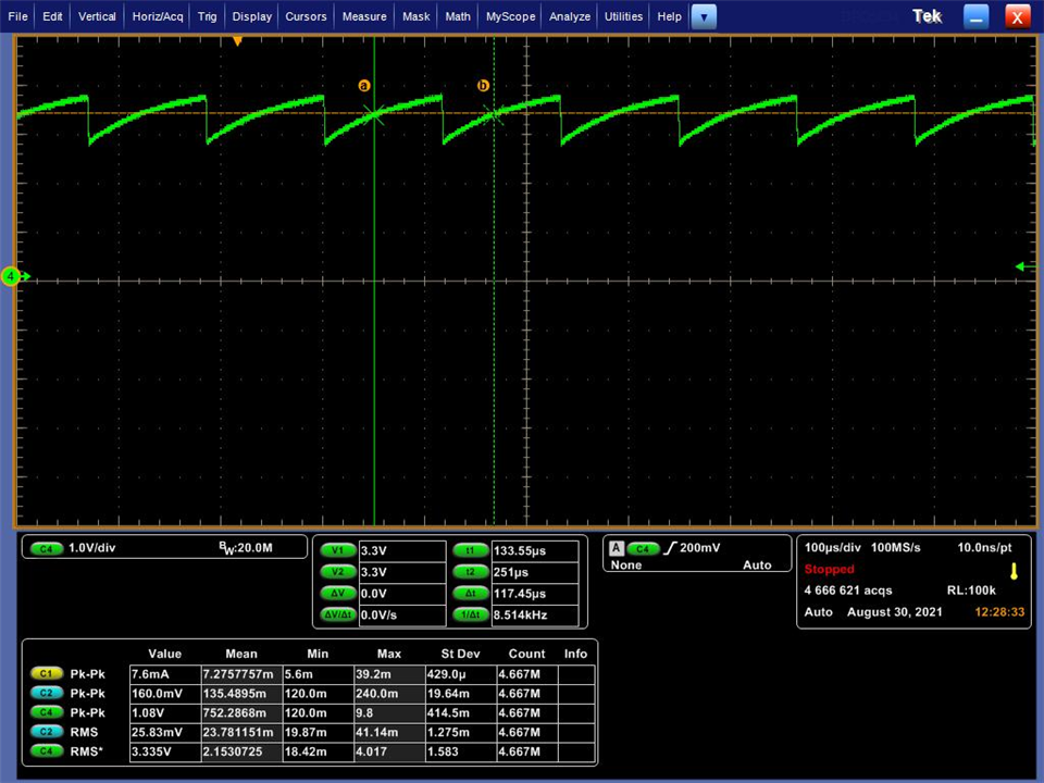
Right now, my biggest lead is an irregularity I noticed when probing the TDI line of the JTAG circuit (see below image).

The switching waveform does not match what I see on other working boards with different processors.

I have verified that it is the processor that is responsible for this behavior by using two different 3.3V power supplies (1 external benchtop, and one on-board buck regulator).

Here is the error report:

[Start: Texas Instruments XDS2xx USB Debug Probe_0]

Execute the command:

%ccs_base%/common/uscif/dbgjtag -f %boarddatafile% -rv -o -S integrity

[Result]


-----[Print the board config pathname(s)]------------------------------------

C:\Users\mblack4\AppData\Local\TEXASI~1\
CCS\ccs1040\0\0\BrdDat\testBoard.dat

-----[Print the reset-command software log-file]-----------------------------

This utility has selected a 560/2xx-class product.
This utility will load the program 'xds2xxu.out'.
The library build date was 'Jun 25 2021'.
The library build time was '16:23:59'.
The library package version is '9.4.0.00129'.
The library component version is '35.35.0.0'.
The controller does not use a programmable FPGA.
The controller has a version number of '13' (0x0000000d).
The controller has an insertion length of '0' (0x00000000).
This utility will attempt to reset the controller.
This utility has successfully reset the controller.

-----[Print the reset-command hardware log-file]-----------------------------

This emulator does not create a reset log-file.

-----[An error has occurred and this utility has aborted]--------------------

This error is generated by TI's USCIF driver or utilities.

The value is '-233' (0xffffff17).
The title is 'SC_ERR_PATH_BROKEN'.

The explanation is:
The JTAG IR and DR scan-paths cannot circulate bits, they may be broken.
An attempt to scan the JTAG scan-path has failed.
The target's JTAG scan-path appears to be broken
with a stuck-at-ones or stuck-at-zero fault.

[End: Texas Instruments XDS2xx USB Debug Probe_0]

  • Michael,

    I've been in contact with Connor C. on this off forum as well, FYI

    Is the noise on TDI present on a fresh device(un-programmed) or only on a device that is running your code? 

    The default configuration of all GPIOs is as input; so if this is showing up a fresh device when the board is powered, then its likely the noise is coupling in from somewhere.

    If this only happens during your code execution, we'll need to look a bit deeper if this is excited by the system when it is running(is there any control loop that matches the 8.514kHz rider frequency in your scope plot) or from the device; the only muxed logic that could be an output on this pin is I2C or PMBUS does your code use either of those modules on the F28004x?

    I'm assuming the other JTAG pins/signals look clean, but would be good to confirm that as well.

    Will look for your reply on the above and go from there.

    Best,

    Matthew

  • Hi Matthew,

    The noise is present on a fresh device (we have not been able to successfully flash this processor yet, actually), and it has actually occurred on multiple fresh devices - to me this indicates that it is related to our design in some way.

    I will see if I can isolate this problem by using a benchtop power supply to power the processor (and turn off all the other on-board power supplies and other peripherals).

    I think I only probed the TDO line, and it also had a similar waveform present on its line.

    I am liking your idea that there may be some noise coupling from somewhere.

    I have some things I want to try now - let me know your thoughts based on the new information I have given you.

  • Michael,

    Agree with your strategy here, a bench supply will prove/disprove if the noise is coming from the PCB power supply. 

    I looked at the MCU page of your schematics and have a few questions:

    1)Can you let me know how the pin VREGENZ is driven(it goes off page).  Is it tied to VSS -> internal VREG is enabled or tied to VDDIO(3.3V) -> internal VREG is disabled

    2)If the internal VREG is enabled, then there is no need for 1.2V supplied externally to the VDD pins.  I noticed that there was a node to 1.2V, but I didn't know if that was to an off-chip voltage source, or just a notation.  If the VREG is enabled and there is also a 1.2V supplied to the pins, I'm not sure the absolute effect on the device other than un-optimal current draw.  I believe the normal VREG is an LDO style so which ever rail is higher will supply the current in case of contention

    3)If the internal VREG is disabled, then you can treat VDDIO_SW as a VDDIO pin, since the switching regulator will not be used.  I noticed there is a ferrite as well as some uF level decap; this won't hurt anything if not used, perhaps there in case it is desired in the future

    4)Want to confirm that the signal VCC_3V3 is the same as VDDIO

    5)Can you comment on the PCB power, is there a 5V main that gets stepped down to 3.3V, etc?  Perhaps if you can share the voltage regulator PN I can take a look at that as well.

    Best,
    Matthew

  • Hi Matthew,

    I have resolve the noise issue on the TDO/TDI lines by using an external power supply to power the 3.3V bus.

    1)Can you let me know how the pin VREGENZ is driven(it goes off page).  Is it tied to VSS -> internal VREG is enabled or tied to VDDIO(3.3V) -> internal VREG is disabled

    VREGENZ is currently floating.

    2)If the internal VREG is enabled, then there is no need for 1.2V supplied externally to the VDD pins.  I noticed that there was a node to 1.2V, but I didn't know if that was to an off-chip voltage source, or just a notation.  If the VREG is enabled and there is also a 1.2V supplied to the pins, I'm not sure the absolute effect on the device other than un-optimal current draw.  I believe the normal VREG is an LDO style so which ever rail is higher will supply the current in case of contention

    We are using the 1.2V internal buck regulator on the chip, so the 1.2V power port is a power source.

    4)Want to confirm that the signal VCC_3V3 is the same as VDDIO

    VDDIO signal comes from pin 47 of the micro, and should read the same voltage (3.3V) as the 3.3V buck regulator we have on board.

    5)Can you comment on the PCB power, is there a 5V main that gets stepped down to 3.3V, etc?  Perhaps if you can share the voltage regulator PN I can take a look at that as well

    We have an external 24V brick, and are bucking that down to 3.3V with the TPS5401

  • Michael,

    Thanks for the update.

    There is a very weak internal pull down on VREGENZ(to enable the MCU's internal VREG/ DC/DC), but I would recommend that you connect this pin directly to ground to ensure it is stable during powerup and operation.  I would re-try the TPS5401 power after you have made this change to see if there is any difference.

    I'd also suggest looking at the XRSn pin when using the TPS5401 to see if you observe the same pulse activity(perhaps with a full rail movement) that you did on the JTAG pins. 

    I'm wondering if we are seeing some localized droop on the VDDIO pins when powering up that is activating the internal voltage supervisor and causing it to pull XRSn low; then go to high as we recover, etc.  That might indicate we need to add more bulk cap on the VDDIO pins, etc.

    Is there a reset supervisor in your design, that also gates XRSn or just a RC to control this timewise with the power up?

    Best,

    Matthew