This thread has been locked.

If you have a related question, please click the "Ask a related question" button in the top right corner. The newly created question will be automatically linked to this question.

TMS320F28022: Error when downloading data to RAM memory using JTAG

Part Number: TMS320F28022

Hello,

I am developing a JTAG system for flashing the TMS320F28022 FLASH memory. I am not using any external debug probes, all hardware and software is developed in-house by my company.
Following your documentation I was able to develop a flashing software that I was able to download and execute to RAM memory of the device.
The device was already programmed and is placed inside a board of a customer (I am not using an evaluation board of yours) so I dumped the memory content and verified the flash content with my flashing software it with success. Then I erased the device and verified the content of the memory behing all 0xFFFF. I was able to access the device until I repowered it.

From that point on I get an error after some words written to RAM memory, I get a C_FAIL from MSR status register (value 0x5). After this error I read the SSR and the value is 0x00573E89.

The steps I am taking are:

  • Reset the device with XRES while holding TRST HIGH;
  • Reset JTAG state machine;
  • Check IDCODE of device (always correct);
  • Write DCSTRBS with 0xAA for connecting debug probe;
  • Halt CPU writing MF_REG0 with EXE_HALT, CND_MASK = 0x3, QUAL_LD;
  • I verify with SSR reading that the EXE_HALT has been set;
  • I write MF_REG0 with just SYNC_LD value set (for clearing of SSR sticky bit);
  • I write DC_STRBS with CRDY_ACT and CRES_ACT (for clearing of SSR sticky bits);
  • I read SSR value being: 0x00572E89;
  • At this point I start writing to RAM with SYS_ACC_W_ADDR16 and SYS_ACC_W_DATA for the two EXSR to be used and the GPSR value associated with EXSR SYS_ACC_W_ADDR16 is address, MU_MUCYC_DATA (0x1), MU_NO_ID, MU_MUHP, MU_MUHPI, MU_MUDBG.

After some words written with this method (remember that I am downloading a flashing software to RAM, starting from 0x8000 address) I get C_FAIL from MSR register as above.

Is there something that I am missing or something that I need to perform in order to avoid this behavior?

If I ignore the C_FAIL error I end up with the device RAM memory (apparently) written with many uncorrect words.

Thank you.

EDIT: I wold like to specify the fact that after IDCODE read, every time that I end up in run-test-idle state I send 16 CLK cycles to the MCU as I read in other threads that this should be done.

  • I made a progress. I wrote to register EMU_BMODE the value 2 (WAIT_BOOT), rebooted the device and wrote to EMU_BMODE the value 0xA (RAM_BOOT) and I am able to boot my software, but there are issues accessing the FLASH memory now.

    The erase operation seems to be performed but it takes a second longer than when the system was programmed and working (3.26s vs 4.26s) and the blank check (verify that all words of flash are 0xFFFF) fails at first word. Reading directly from device flash results in first 0x1000 words of Flash being values different from 0xFFFF (edit: testing again i see 0x0000 as value for first 0x1000 words of flash). From 0x3F5000 on all words are 0xFFFF.

    Do you know what can cause this issue? Any hints about what to look for in the first place?

    Thank you.

  • Andrea,

    Thanks for reaching out to the TI E2E, we're still working on getting the correct engineer assigned to your question.  Appreciate your patience here, will try and get a response before the weekend.

    Best,

    Matthew

  • Thank you Matthew,

    Just this morning I solved the problem with FLASH readback but still I have issues with the process of executing my software downloaded to the target's RAM.

    I download the software to RAM, then I write EMU_BMODE with 0xA and write the MF_REG0 in order to HALT the CPU and after this I write the IC register of the CPU with the entry point for my application and then write MF_REG0 with EXE_COND for starting the execution of my software. What I see is that if I read back the IC register the IC has moved forward in my code (even if the core should be in HALT state). This puzzles me.

    I will wait for an engineer helping me.

    Thank you again.

  • Hi Andrea,

    Please could you confirm at what point was the IC read back? Was it before or after the EXE_COND was issued? Also, what address was written to IC and what was read back?

    Are you still seeing the CFAIL issue or has that been resolved?

    Thanks,
    Ashwini

  • Hello Ashwini,

    the read back was before issuing EXE_COND. I wrote 0x8000 and read back something further in my code e.g. 0x8230.

    But I discovered that there was a problem triggering the XRST line of the MCU due to the board's design. I solved the problem and used the GPIOs to enter in WAIT mode. Now the problems are mitigated but I see somehow some instabilities sometimes.

    The CFAIL issue seems to be solved by entering WAIT mode.

    I needed to work on another project in parallel, once I will get back to the TMS320 I will update about the instability problem.

    Thank you.

  • Hi Andrea,

    Thanks for the update.

    Regards,
    Ashwini

  • Sorry for the long wait, I had to take care of other aspects of the project meanwhile.

    I have come back to the TMS320 programming and I am facing again issues. I programmed the target MCU with a wrong firmware and now I want to recover it flashing the correct one. The problem is that I cannot write to RAM correctly.

    My approach is to set the PINs for the WAIT_BOOT mode and enter in this mode, download the flashing software to RAM and then move the IC register to the start of my software, then run with EXE_COND.

    My problem now is that when I try to read back the value I should have written to RAM, I can only read 0x00 as a value. There is no CFAIL set during the writing procedure to RAM.

    What could it be now? I tought that the WAIT mode of the MCU should not lead to any side effect of a wrong FW written to flash.

    Thank you.

  • Hi Andrea,

    When device enters WAIT_BOOT mode, can you confirm that the address the core is halted at is the boot location where the device loops on ESTOP0 instruction? Also can the SSR be scanned out at this point to read back the system state? This may give some clues.

    Thanks,
    Ashwini

  • Hello Ashwini,

    I think I have figured out the problem, but not the solution yet. The file for programming was loaded in an uncorrect way and a password was programmed for the CSM. Indeed for example I can read/write data from 0x50 RAM0 memory but not from 0x8000 (protected by CSM).

    I can replicate the error in order to obtain the unlocking password, but I have not yet made a SW to be run from a unprotected RAM area. Is it possible to unlock the CSM writing directly to its registers using JTAG, without a need of a SW to be run from RAM? Where is the CSM located in the memory map area?

  • Hi Andrea,

    Let me find out from the CSM expert and let you know.

    Thanks,
    Ashwini

  • Andrea,

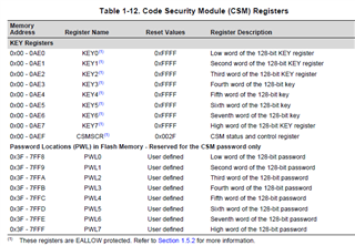
                I think you have a locked device with unknown password. If true, you have to replace the part. No other option. Below are the memory-mapped locations concerning CSM (Basically just the password locations in flash and the KEY registers): (from page 52 of SPRUI10)

  • Hello Haaresh,

    thank you for your answer. I got to the same conclusion at the end, I will have another sample board for testing soon so that I could continue with this work.

    I hope that no other problem arises at this point. I will share the situation after my tests.

  • Hi Andrea,

    Sounds good.

    Thanks,

    Ashwini

  • Hello,

    I received and tested the new board. Now I can perform most of the time the programming of the device correctly. Seldomly I saw the verify of the flash memory content fails.
    The download software that I designed is downloaded to address 0x8000 and I reserved the RAMM0 memory at 0x50 for two data buffer, each of 768 Bytes.

    I noticed that it seems that the MCU reads some wrong data from the RAMM0 memory sometimes. I replaced the verify function with a 16 bit checksum calculation and comparison with the same checksum calculated inside the programmer. I get it constantly failing as the MCU at a certain point calculates a wrong checksum.
    My guess is that the data written via JTAG is not instantly written to memory and the MCU reads some wrong byte from memory or that there is some kind of cache memory.

    Do you have some hint about what could cause an issue like this? And why if it is always happening with the checksum calculation and just very rarely with the verify routine?

    Also, if I perform the checksum calculation AFTER the verify routine is called, the checksum result is correct, so it is not a transmission error issue.

    Thank you.

    Best regards.

  • Hi Andrea,

    The device does not have a cache so the issue seems to be something else. Is the checksum being calculated and verify being called on the Flash memory being programmed or the RAMM0 buffer?

    Thanks,

    Ashwini

  • Hi Ashwini,

    The checksum is calculated reading from RAMM0 and the FLASH verify at the moment is performed with FLASH API and passing a pointer to the buffer present in RAMM0 (the same for which the checksum is calculated) for comparison with values in flash.

    I also tried to perform a verify comparing data read from RAMM0 and from FLASH. With both API and this method the error is very rare.

    Also, if I just execute the checksum or verify (no previous erase, blankcheck and program) the error does not occur. It just occurs after a Erase, blankcheck and program. I am using the API provided by you of course and I dumped the content of the MCU in order to check that the memory content is correct.

    If you need some other detail let me know.

    Thank you!

  • Andrea,

    Can you check the value you are using for the flash WS and make sure it is correct for the speed the device is clocked at? 

    For instance at 60MHz the paged and random WS should = 2 and the OTP WS should = 3.

    In either case does increasing the WS make any difference to a checksum failure occurring?

    Best,
    Matthew

  • Hello Matthew,

    I found uncorrect values in the "f2802x_sysctrl.c" file provided with example for the WS. Also, the 50MHz (as my device is clocked at 50MHz) was not present. I added this code:
        #elif (CPU_FRQ_50MHZ)
        // Set the Paged Waitstate for the Flash
        //
        FlashRegs.FBANKWAIT.bit.PAGEWAIT = 1;

        //
        // Set the Random Waitstate for the Flash
        //
        FlashRegs.FBANKWAIT.bit.RANDWAIT = 1;

        //
        // Set the Waitstate for the OTP
        //
        FlashRegs.FOTPWAIT.bit.OTPWAIT = 2;

    But this has not changed the behavior. I could try to rise this values but I don't see what could it change since the checksum is calculated with values stored inside RAMM0 and not in flash.

    I calculate the checksum for the transmitted buffer inside the programmer, I send it to the MCU together with the buffer and I make the MCU calculate the same checksum using this transmitted buffer stored in RAMM0.

    There are two structured buffers in RAMM0, for each buffer I have a field for marking the operation as "done" and I this field before overwriting the buffer with the new one and going on with the next operation. I see that the first buffer's checksum is correctly computed but the second buffer's checksum is wrongly computed. Maybe the problem could be arising because I am writing a location of RAMM0 while the MCU is accessing another location of RAMM0?

    If I write a buffer and wait for the completion mark before going on writing the second buffer, the issue does not occur.

    Thank you.

  • Andrea,

    Thanks for the clarification I had missed that everything is in RAMM0 in this case(I thought you were re-fetching from the flash post program, hence the WS suggestion). 

    Since we using JTAG to scan into the memory, the test tap will look for spare cycles to operate while the CPU is executing as well.  Since we are actively reading the 1st buffer in M0, and trying to write to it with the test tap I could see where it would be hard to predict exactly when the writes would happen.  That doesn't mean that we should miss a write or have a bad write per se, just might be delayed more than we think. 

    I'm not certain that with the JTAG insertion that the pipeline protection that is part of normal operation is guaranteed (meaning that since the Write phase of the CPU pipeline is last, if the CPU decodes a read to the same location it would stall it normally.).  Since the JTAG is inserting these writes in the holes in program execution, the protection may be bypassed here, causing your issues. 

    This would align to your passing condition, where you wait until the completion mark to overwrite.  Would it be possible to create a ping/pong type buffer so the addresses don't overlap so you could get back the throughput?

    Best,

    Matthew

  • Thanks Matthew,

    at the moment I am already using a ping-pong style buffering type, if we mean the exact same approach. I will explain better:

    I split RAMM0 in two parts for two buffers, each with an associated header that contains auxiliary data as command to be executed, address for operation, etc.. and also a field for flags. Once the flag for a buffer is marked as "Go for execution" our programmer will not write that buffer, but it will wait for the MCU to perform the associated operation and for it to mark the flag as "Execution complete". Once the execution is marked as completed, the programmer reads the answer (pass or failure and auxiliary information) and if the status is "OK" it overwrites the buffer and the associated auxiliary fields. This is a standard approach we use also for other MCU types.

    So I think that there is no "logical" risk for the MCU and programmer to go out of sync, but maybe could it be that some JTAG write operation are completed before others even if their order should be different? Like, I write the complete data buffer for checksum with JTAG and after that I write with JTAG the "GO" flag, but the GO flag is visible for the MCU before the full array of data of the buffer has been actually overwritten?

    Thank you again.

  • Andrea,

    I will need to check, I would assume the order of the operations is maintained, if we are talking about all writes to the buffer, then a final write to a flag location this shouldn't shuffle around in time. 

    Just to confirm that the header is contained in RAM?

    I'm going to ping someone in the tools team to see if this is something they have ran into, or there is some step I am not thinking of with respect to the C28x.

    Best,

    Matthew

  • Hello Matthew,

    yes, all is contained in RAM memory, since my goal is to program the FLASH memory, the only thing that I write to it is just the firmware to be stored.

    Thank you, I will wait for a reply.

    Best regards

    P.S. Sorry, I flagged the answer as "This solved my issue" as a mistake!

  • Andrea,

    Wanted to let you know we are still investigating this, please give us another day to get back with you.

    Best,

    Matthew

  • Hi Andrea,

    One quick question to understand the setup, is real-time mode enabled or disabled in the JTAG setup?

    Thanks,

    Ashwini

  • Hello Ashwini,

    sorry for the delay. I do not write MF_REG0 real time related bit after debug reset and I read BIT 2 of MSR as 1, so I should be in real-time mode based on documentation.

    Thank you.

  • Hi Andrea,

    Can you disable real-time mode and see if that resolves the MCU out of sync issue?

    Thanks,
    Ashwini

  • Hello Ashwini,

    I tried to disable the real-time mode (wrote MF_REG1 and verified that MSR RT bit was set to 0) but this has not changed the behavior. Still the issue remains.

    Best regards.

  • Andrea, both Ashwini and Matthew are currently out of the office.  You should receive a reply by Wednesday.  Thank you for your patience.

    Regards, Joe

  • Hi Andrea,

    I can think of a 2 other checks:

    1. Set MF_REG_0:CND_MSK[0] = 1 and  CND_MSK[1] = 1 to ignore HPI and DBGM when performing the JTAG access

    2. Ensure that after each JTAG scan the Run-Test-Idle is being held for at least 20 TCLKs.

    Sorry about the lack of quick resolution here, our in house tools do not use double buffering and hence we have not run into this issue. Thanks for your patience.

    Thanks,

    Ashwini

  • Hello Ashwini,

    I understand the complexity of debugging such a kind of issue, no problem.

    In any case, I tried both your suggestions (also I raised up gradually to 128 TCLKs for testing) but the same issue remains.

    Best regards.

  • Hi Andrea,

    Thanks Andrea. Can you confirm that you are seeing no fails in the MSR nor is the SSR showing any unexpected status?

    In the meanwhile I will reach out to other experts as well.

    Thanks,

    Ashwini

  • Hello Ashwini,

    I cannot 100% confirm this, because if I perform controls over MSR or SSR the writings get delayed and thus the error does not occur (but the programming times rise quite a lot). What I can say is that I don't think there are CFAIL errors in MSR because the error always occurs if I try to perform the checksum before verifying the data but very rarely when I compare the data with values in flash.

    Also, serializing the two buffer writings (writing one, waiting for operation to complete, writing the second, waiting complete etc...) seems to completely clear the issue. Programming times stay low, but I would like to figure out the root cause of the behavior since it could maybe emerge in different scenarios using a different MCU sample.

    Best regards.

  • Hi Andrea,

    Thanks for the reply.

    I got a good tip from the team - What address is the Stack Pointer set at? On reset the SP is set at M1 (see device datasheet for this information). It could be that the buffers are overlapping the stack and hence we see the issue at run time? Could you try placing the double buffers in some other RAM and not M0, M1 but keep SP at M1.

    If the above also does not resolve the issue, can you do an experiment where the CPU code runs a simple wait loop during JTAG download to RAM and see if the issue goes away. This is just to check and see if the problem is because of JTAG and CPU simultaneously accessing RAM.

    Thanks,

    Ashwini

  • Hi Andrea,

    Also do note that C28 is not byte addressable. So if you have a buffer defined with the byte/char/8-bit type, it will actually be a buffer of 16-bit word type.

    Thanks,

    Ashwini

  • Hello Ashwini,

    regarding buffer placement and overlapping with stack, I think that is not the case. I place buffer starting from 0x50 (RAMM0) and the summed size of the two buffers does not go up to 0x400, where the stack bottom is placed. I noticed that the stack is placed at 0x400 and grows upwards (I am used to the opposite) but in any case I read the value of the SP during the failure being 0x41E, no it is not pointing to any address occupied by the buffers.

    Regarding the addressing I am aware of that, I use a uint16_t buffer and I am counting words instead of bytes for the size of the operations (and addresses).

    Regarding the looping when the data is being transfered I almost do this when I wait for each operation to be completed. I explain it better: since after the operation has been completed the software writes the "finished" flag and then it enters a loop waiting for the next "go" flag, the CPU is in a state of loop waiting for the programmer to signal that a buffer has been transfered. Indeed, as said, waiting for every operation to complete before writing the next buffer seems to solve all the issues, but this of course is cutting all the benefits of having 2 buffers managed as ping-pong buffers.

    Thank you for your help.

    Best regards.

  • Hi Andrea,

    Thanks a lot for the details, I am taking this feedback to the team to see if we can offer any other suggestions.

    Thanks,

    Ashwini

  • Hi Andrea,

    Which RAM is the code being placed in?

    Can we do this experiment - separate the buffer into 2 memory banks - keep Buffer A in M0 RAM but put Buffer B at L0 SRAM - separating the buffer into 2 memory banks will help determine if there is a conflict with core and debug accessing the same memory bank if this works.

    Thanks,

    Ashwini

  • Hello Ashwini,

    sorry for the very late reply. The time for the project has ended and I decided to stick with the wait for each buffer ending (so like using only one buffer). Next time I'll need to develop a download software for another TMS320 device, I will try your latter suggestion if the problem arises again. At the moment I have no time for further tests (as this test requires me to edit a substantial part of the code).

    Answering your question: the code is placed in PRAML0 area and buffers in RAMM0 at the moment.

    Best regards.

  • Hi Andrea,

    Thanks for the update.

    Regards,

    Ashwini