This thread has been locked.

If you have a related question, please click the "Ask a related question" button in the top right corner. The newly created question will be automatically linked to this question.

TMS320F2808: Spi Mode 1 or 3 timing issues

Part Number: TMS320F2808

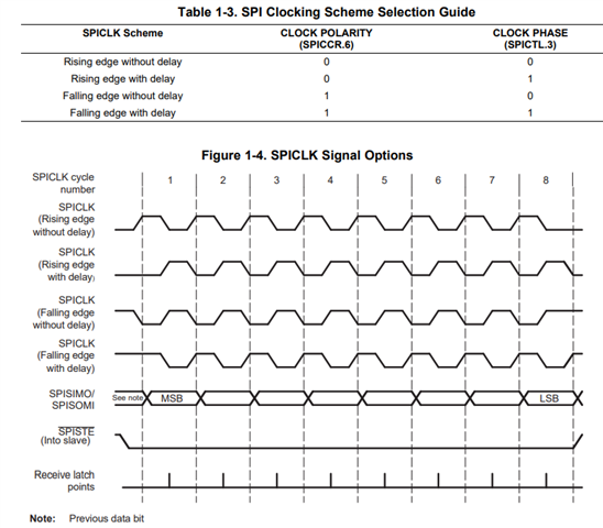
I have a device that requires SPI mode 3 connected to my F2808 dev kit. (I have another device with SPI mode 0 and works great.)

The same issue exists for both SPI mode 1 or 3 so I will focus on SPI mode 1 and I am sure the issue will also be resolved for SPI Mode 3.

One other setup is that the data is in 4-bit mode (SPICCR.bit.SPICHAR) so the data shifting is considered. The data I will focus on is the F2808 sending a 0x901B4 to the external device.

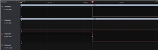
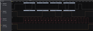
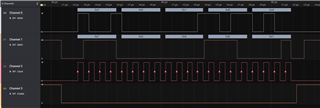
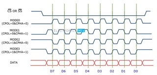
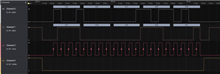
When in SPI Mode 0 or 2, the data shifts out as expected. See the TMC262_SPI_Mode0 attached image. However, when the SPI mode is changed to 1 or 3, the first SPI clock is occurring EXACTLY as the first data bit is transitioning from a high to a low of the 0x9 (1001b) and therefore is recognized as a 0 and then the rest of the data is off by 1 bit. See the TMC262_SPI_Mode1 image attached.

There is no difference in the clock setups as all device run a 1MHZ (SPIBRR = 0x0009, SysCtrlRegs.HISPCP.all = 0x0005, SysCtrlRegs.LOSPCP.all = 0x0005, SysCtrlRegs.XCLK.bit.XCLKOUTDIV=2).

Is there some setup I am over looking? The GPIO setup for the port is as follows:

    GpioCtrlRegs.GPAPUD.bit.GPIO20 = 0;   // Enable pull-up on GPIO20 (SPISIMOC)
    GpioCtrlRegs.GPAPUD.bit.GPIO21 = 0;   // Enable pull-up on GPIO21 (SPISOMIC)                                                                                                             
    GpioCtrlRegs.GPAPUD.bit.GPIO22 = 0;   // Enable pull-up on GPIO22 (SPICLKC)                                                                                                             
    GpioCtrlRegs.GPAPUD.bit.GPIO23 = 0;   // Enable pull-up on GPIO23 (SPISTEC)                                                                                                             
    
/* Set qualification for selected pins to asynch only */
// This will select asynch (no qualification) for the selected pins.
// Comment out other unwanted lines.

    GpioCtrlRegs.GPAQSEL2.bit.GPIO20 = 0;   // Sysclock sync GPIO20 (SPISIMOC)
    GpioCtrlRegs.GPAQSEL2.bit.GPIO21 = 0;   // Sysclock sync GPIO21 (SPISOMIC)
    GpioCtrlRegs.GPAQSEL2.bit.GPIO22 = 0;   // Sysclock sync GPIO22 (SPICLKC)
    GpioCtrlRegs.GPAQSEL2.bit.GPIO23 = 0;   // Sysclock sync GPIO23 (SPISTEC)

/* Configure SPI-C pins using GPIO regs*/
// This specifies which of the possible GPIO pins will be SPI functional pins.
// Comment out other unwanted lines.

    GpioCtrlRegs.GPAMUX2.bit.GPIO20 = 2;   // Configure GPIO20 as SPISIMOC
    GpioCtrlRegs.GPAMUX2.bit.GPIO21 = 2;   // Configure GPIO21 as SPISOMIC     
    GpioCtrlRegs.GPAMUX2.bit.GPIO22 = 2;   // Configure GPIO22 as SPICLKC    
    GpioCtrlRegs.GPAMUX2.bit.GPIO23 = 2;   // Configure GPIO23 as SPISTEC  

  • Hi Jeffery,

    Can you please describe what spi modes you are referring to? Also, the differences in the actual software configuration between the modes?

    Best Regards,

    Marlyn

  •     switch(spimode)
        {
        /*
         *    Mode   CLKPOL   PHASE
         *      0       0       0   // All data transitions are during the rising edge,
         *                               non-delayed clock. Inactive level is low.
         *      1       0       1   // All data transitions are during the rising edge,
         *                               but delayed by half clock cycle. Inactive level is low
         *      3       1       0   // All data transitions are during the falling edge.
         *                               Inactive level is high
         *      2       1       1   // All data transitions are during the falling edge,
         *                               but delayed by half clock cycle. Inactive level is high
         *  SPICCR.bit.CLKPOLARITY (.6) 0 Data is output on rising edge and input on falling edge
         *  SPICCR.bit.CLKPOLARITY (.6) 1 Data is output on falling edge and input on rising edge
         *  SPICTL.bit.CLK_PHASE   (.3) 0 Normal SPI clocking scheme, depending on the CLOCK POLARITY bit (SPICCR.6)
         *  SPICTL.bit.CLK_PHASE   (.3) 1 SPICLK signal delayed by one half-cycle; polarity determined by the CLOCK POLARITY bit
         */
        default:
        case Mode0:
            // Setup for Mode 0
            spiregs->SPICCR.bit.CLKPOLARITY = 0;
            spiregs->SPICTL.bit.CLK_PHASE = 0;
            break;
        case Mode1:
            spiregs->SPICCR.bit.CLKPOLARITY = 0;
            spiregs->SPICTL.bit.CLK_PHASE = 1;
            break;
        case Mode2:
            spiregs->SPICCR.bit.CLKPOLARITY = 1;
            spiregs->SPICTL.bit.CLK_PHASE = 0;
            break;
        case Mode3:
            spiregs->SPICCR.bit.CLKPOLARITY = 1;
            spiregs->SPICTL.bit.CLK_PHASE = 1;
            break;
        }

  • Hi Jeffrey,

    Thank you for the information above. The reason I ask is because there may not be standardization for spi "modes" between our devices and other devices. Have you confirmed that the other external device matches the same descriptions with our device in terms of clock polarity and phase?

    For your reference:

    Could you also please reattach the images with the naming convention individually? Our system doesn't track that information. 

    Best Regards,

    Marlyn

  • I am trying to confirm with the customer regarding what Mode 3 is to them but I feel they may be expecting the following format:

    So is there a way to setup CPOL of 1 but CPHA rising edge without delay? (I feel you may be on track as to what is Mode 3 for the customer doesn't mean is Mode 3 to the F2808.)

    TMC262_SPI_Mode0 image

    TMC262_SPI_Mode1 image

  • Hi Jeffrey,

    I am trying to confirm with the customer regarding what Mode 3 is to them but I feel they may be expecting the following format:

    Thank you, this may help clear up what is going on.

    So is there a way to setup CPOL of 1 but CPHA rising edge without delay?

    Unfortunately, no. The only configurable options are the ones in the table I provided in the previous reply. Comparing the diagram you provided and the one for F2808, mode 3 and 1 are different due to the delay the F2808 provides.

    Best Regards,

    Marlyn

  • Thank you as that explains it. Now I just need to see if the customer only accepts the Mode 3 in the image I provided and if so, then their product will not be be SPI compatible with the F2808.