This thread has been locked.

If you have a related question, please click the "Ask a related question" button in the top right corner. The newly created question will be automatically linked to this question.

LAUNCHXL-F28069M: spi

Part Number: LAUNCHXL-F28069M
Other Parts Discussed in Thread: C2000WARE

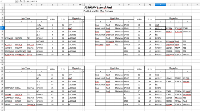
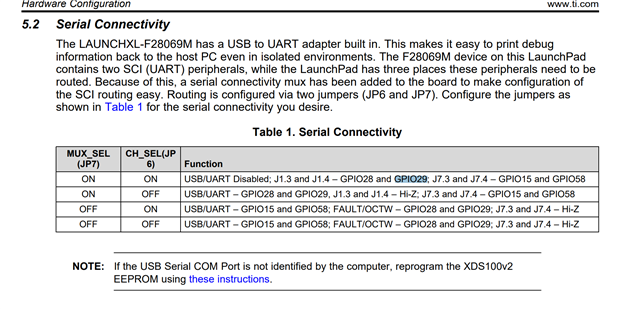
I was following the Example_2806xSci_Echoback.c example in the ti device support.  I have an XBee radio module that I am receiving data from and I want to relay that to my f28069M board.  I connected jumper wires from the xbee to the GPIO28 and GPIO29 pins, but I do not see anything coming in. Can this echoback example be used like that or would there be another way to go about what I am trying to do?  Ultimately, I am trying to get input from a remote and spin a motor. However, at this moment, I am just trying to get values to display in the serial console and have them change when I move the joystick around.  

  • Charlie,

    The echoback example only echo's characters that the device receives. If nothing is sent to the device it will not respond. And it certainly will not respond in any specific format. you will need to make modifications to this code to suit your purpose.  

    From a HW perspective, for SCI: connect TX to RX and RX to TX. You should also connect a ground wire between the devices to give them a common reference.

    From a SW perspective you need to configure the SCI frame to match the XBee's format and configure the same baud rates.

    Its unclear if you're trying to use SPI, as indicated in the title, or SCI, as mentioned in the post, but please know that these are very different.

    It is also unclear what your serial console is, Please note that you cant just mash a bunch of serial nodes onto a bus and expect everything to work, SCI is not intended to have multiple drivers operating at random.

    Good luck,
    Cody 

  • Thank you for the response.  So yes I am trying to transmit serial data via SCI. So I have the f28069m board plugged into my computer through the usb => usb-b cable and I connected to the port using putty. So through the SCI echo back example it was transmitting serial data through the usb.  Tonight, I used a salae logic analyzer and hooked a channel up to the TX GPIO29 and modified the code to just keep outputting "Hello" over and over, but I still saw no data in my logic 2 software.  

    Here is the main function

    void main(void)
    {
        Uint16 ReceivedChar;
        char *msg;
    
        //
        // Step 1. Initialize System Control:
        // PLL, WatchDog, enable Peripheral Clocks
        // This example function is found in the F2806x_SysCtrl.c file.
        //
        InitSysCtrl();
    
        //
        // Step 2. Initalize GPIO:
        // This example function is found in the F2806x_Gpio.c file and
        // illustrates how to set the GPIO to its default state.
        //
        //InitGpio(); Skipped for this example
    
        //
        // For this example, only init the pins for the SCI-A port.
        // This function is found in the F2806x_Sci.c file.
        //
        InitSciaGpio();
    
        //
        // Step 3. Clear all interrupts and initialize PIE vector table:
        // Disable CPU interrupts
        //
        DINT;
    
        //
        // Initialize PIE control registers to their default state.
        // The default state is all PIE interrupts disabled and flags
        // are cleared.
        // This function is found in the F2806x_PieCtrl.c file.
        //
        InitPieCtrl();
    
        //
        // Disable CPU interrupts and clear all CPU interrupt flags
        //
        IER = 0x0000;
        IFR = 0x0000;
    
        //
        // Initialize the PIE vector table with pointers to the shell Interrupt
        // Service Routines (ISR).
        // This will populate the entire table, even if the interrupt
        // is not used in this example.  This is useful for debug purposes.
        // The shell ISR routines are found in F2806x_DefaultIsr.c.
        // This function is found in F2806x_PieVect.c.
        //
        InitPieVectTable();
    
        //
        // Step 4. Initialize all the Device Peripherals:
        // This function is found in F2806x_InitPeripherals.c
        //
        //InitPeripherals(); // Not required for this example
    
        //
        // Step 5. User specific code
        //
        LoopCount = 0;
        ErrorCount = 0;
    
    //    scia_fifo_init();	   // Initialize the SCI FIFO
    //    scia_echoback_init();  // Initalize SCI for echoback
    
    //    msg = "\r\n\n\nHello World!\0";
    //    scia_msg(msg);
    //      msg = "Initialized!\0";
    //      scia_msg(msg);
    //
    //    msg = "\r\nYou will enter a character, and the DSP will echo it back! \n\0";
    //    scia_msg(msg);
    
        for(;;)
        {
    //        msg = "\r\nEnter a character: \0";
    //        scia_msg(msg);
    
            msg = "Hello\0";
            scia_msg(msg);
            //
            // Wait for inc character
            //
    //        while(SciaRegs.SCIFFRX.bit.RXFFST !=1)
    //        {
    //            //
    //            // wait for XRDY =1 for empty state
    //            //
    //        }
    
            //
            // Get character
            //
    //        ReceivedChar = SciaRegs.SCIRXBUF.all;
    
            //
            // Echo character back
            //
    //        msg = "  You sent: \0";
    //        msg - " Char received from remote : \0";
    //        scia_msg(msg);
    //        scia_xmit(ReceivedChar);
    
            LoopCount++;
        }
    }

    init function for the gpio registers

    void
    InitSciaGpio()
    {
        EALLOW;
    
        //
        // Enable internal pull-up for the selected pins
        // Pull-ups can be enabled or disabled disabled by the user.
        // This will enable the pullups for the specified pins.
        //
        GpioCtrlRegs.GPAPUD.bit.GPIO28 = 0;  // Enable pull-up for GPIO28 (SCIRXDA)
        //GpioCtrlRegs.GPAPUD.bit.GPIO7 = 0;  // Enable pull-up for GPIO7 (SCIRXDA)
    
        GpioCtrlRegs.GPAPUD.bit.GPIO29 = 0;	 // Enable pull-up for GPIO29 (SCITXDA)
        //GpioCtrlRegs.GPAPUD.bit.GPIO12 = 0; // Enable pull-up for GPIO12 (SCITXDA)
    
        //
        // Set qualification for selected pins to asynch only
        // Inputs are synchronized to SYSCLKOUT by default.
        // This will select asynch (no qualification) for the selected pins.
        //
        GpioCtrlRegs.GPAQSEL2.bit.GPIO28 = 3;  // Asynch input GPIO28 (SCIRXDA)
        //GpioCtrlRegs.GPAQSEL1.bit.GPIO7 = 3;   // Asynch input GPIO7 (SCIRXDA)
    
        //
        // Configure SCI-A pins using GPIO regs
        // This specifies which of the possible GPIO pins will be SCI functional 
        // pins.
        //
        
        //
        // Configure GPIO28 for SCIRXDA operation
        //
        GpioCtrlRegs.GPAMUX2.bit.GPIO28 = 1;
        
        //
        // Configure GPIO7  for SCIRXDA operation
        //
        //GpioCtrlRegs.GPAMUX1.bit.GPIO7 = 2;
    
        //
        // Configure GPIO29 for SCITXDA operation
        //
        GpioCtrlRegs.GPAMUX2.bit.GPIO29 = 1;
        
        //
        // Configure GPIO12 for SCITXDA operation
        //
        //GpioCtrlRegs.GPAMUX1.bit.GPIO12 = 2;
    
        EDIS;
    }

    Interrupts called in the main function

    void
    scia_echoback_init()
    {
        //
        // Note: Clocks were turned on to the SCIA peripheral
        // in the InitSysCtrl() function
        //
        
        //
        // 1 stop bit,  No loopback, No parity,8 char bits, async mode,
        // idle-line protocol
        //
        SciaRegs.SCICCR.all =0x0007;
        
        //
        // enable TX, RX, internal SCICLK, Disable RX ERR, SLEEP, TXWAKE
        //
        SciaRegs.SCICTL1.all =0x0003;
    
        SciaRegs.SCICTL2.bit.TXINTENA = 0;
        SciaRegs.SCICTL2.bit.RXBKINTENA = 0;
    
        //
        // 9600 baud @LSPCLK = 22.5MHz (90 MHz SYSCLK)
        //
        SciaRegs.SCIHBAUD    =0x0001;
        SciaRegs.SCILBAUD    =0x0024;
    
        SciaRegs.SCICTL1.all =0x0023;  // Relinquish SCI from Reset
    }
    
    //
    // scia_xmit - Transmit a character from the SCI
    //
    void
    scia_xmit(int a)
    {
        while (SciaRegs.SCIFFTX.bit.TXFFST != 0)
        {
            
        }
        SciaRegs.SCITXBUF=a;
    }
    
    //
    // scia_msg - 
    //
    void
    scia_msg(char * msg)
    {
        int i;
        i = 0;
        while(msg[i] != '\0')
        {
            scia_xmit(msg[i]);
            i++;
        }
    }
    
    //
    // scia_fifo_init - Initalize the SCI FIFO
    //
    void
    scia_fifo_init()
    {
        SciaRegs.SCIFFTX.all=0xE040;
        SciaRegs.SCIFFRX.all=0x2044;
        SciaRegs.SCIFFCT.all=0x0;
    }

  • Look at SW3 in the schematic. It has the ability to break the RX line. you can find the schematic in C2000Ware.

    I believe the default Putty configuration should work well with this example, the default example looks to be configured for a baud of 9600. Just select serial communications and the correct COM port and it should work.

    Once the putty terminal is open press a key on your keyboard and the device will respond with something along the lines of "you typed : A" .

    Regards,
    Cody 

  • I can see the output just fine in putty and the sample program runs fine.  I can see it prompt me and then echo back what I type.  However, I am trying to just write a simple program to output data to the tx pin and see it on my logic analyzer.  I am trying to determine which pins are the tx and rx pins on the f28069m and hook the tx pin up to the logic analyzer and see data coming out.  I want to connect an xbee module's tx and rx pins to the boards tx and rx pins. I looked at the excel like spreadsheet of the pinout, but do not see the gpio 29 or gpio 28 listed there.  


    In the f28069m user guide there is this:

    and I thought maybe the gpio28 and gpio29 pins correlated to the j1.3 and j1.4 pins, but each place that I put my logic analyzer wire, I see no activity.  
    I am software developer, so this is all new to me.  I took an embedded systems class at university, but it has been awhile.  I remember some stuff, but not very well.  Is there better documentation that can show me how the pins map and or how to program this board?  I see all of the examples, but I am not finding them of much use or I am just using them incorrectly.  

    In the code above, you can see I commented out all the code and was just trying to send a message over and over to the tx pin.  I assume it was doing it, but for my sanity I would like to see it on my logic analyzer.  I would think that the program is working, but I'm just on the wrong pin.   

    Does my above program seem like it is going to output data to the tx pin? And maybe I'm not seeing the data because my logic analyzer wire is just on the wrong pins?

    Do you know which pins correlate to the gpio28 and gpio29?

  • Ah, If you are using a Launchxl- F28069M EVM please disregard my last statement, it was operating under the assumption you were using the controlCARD.

    You have correctly determined that the GPIOs do not directly connect to any pins. Pins J1.3 and J1.4 correlate to GPIO28 and GPIO29 respectively. This connection is not always made, it depends on JP6 and JP7's configuration. The table you have copied has been provided to simplify the configuration, but if you look at the schematic you'll see some Muxs which can control this connection. Your SW is already bringing the data to the GPIO pin, the mux needs to be configured to bring that signal from the c2000 device to the Jx header that you're trying to observe.

    Set JP7 and JP6 correctly and you should see the data on the pins.

  • Thanks so much!  I was reading that chart wrong and once I put both jumpers on and modified the code a little I can see data coming off of the tx pin.