Hi there,
I have two prototype boards made with this TI micro and am unable to connect to this device using the XDS100V3 debugger. I get the message: "The JTAG IR and DR scan-paths cannot circulate bits, they may be broken."
I am unsure whether my boards are functioning properly as with one of them VDD seems to gradually drop below 1.2V until it hits 0.8V. XRSn reset pin is measured at 3.3V which looks right.
On the other board VDD is stable at around 1.2V but the XRSn reset pin seems to be pulling itself down to a constant 0.5V (I read somewhere this device can drive this pin low in the event of an internal issue).
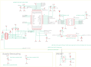
See my circuit below, the only difference I see between the recommended layout is I do not have a capacitor between VREFHI and VREFLO as I am not using the ADC.
I have set the boot mode to SCI / Wait Boot which I assume is correct for flashing/debugging?
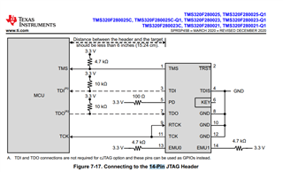
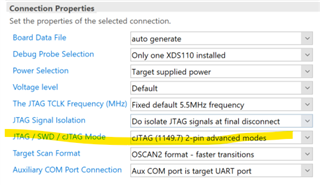
Another thing that comes to mind is that this JTAG 14-pin interface recommends leaving the TRST pin unconnected on the header as per the below. I wonder if the XDS100V3 is not happy with this lack of ground/VCC on this pin?
I get the same message trying to flash either board. The 3.3V supplies look fine when measured. I am not sure how to solve this issue and any input would be appreciated.
Thanks in advance for your help.