This thread has been locked.

If you have a related question, please click the "Ask a related question" button in the top right corner. The newly created question will be automatically linked to this question.

TMS320F28020: Software Reset via Watchdog Control Register

Part Number: TMS320F28020
Other Parts Discussed in Thread: C2000WARE

Hi All,

Current project needs sw reset feature.  Previous iteration (microchip MCU) used a GPIO pin to pull its own reset pin low.  This approach hasn't worked with the 28020.  First off the GPIO pin is low at startup, so the MCU never comes out of reset.  Placing an inverter in series allows boot, but when trying to assert the pin high, it starts to rise then hangs at milliVolts.

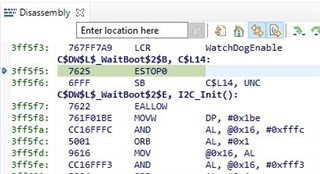
Now I'd like to use the WDT feature to cause a reset. I've read a couple of threads that refer to setting the WDCR to an illegal state.  Adding a line that does just that results in code going off into the weeds.  Stepping through the code, I see in the disassembly window that the program has halted on an estop, but I'm not sure how it gets there.

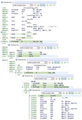
Here's the snippet of code that causes the error:

if(val1 == 9)
{
    if(resetFlag_CPU)
    {
        resetFlag_CPU = 0;

        EALLOW;
        DINT;

        myWDog->WDCR = 0x17;    // 0X17 Keeps div by in lower 3 bits and adds faulty check bit

        EINT;
        EDIS;
    }
}

With line 10 (above) commented out, code works fine.  When it's not commented out, the code executes seemingly as expected, the function it's running in completes and returns, but that's when it runs to estop.

It's my intent to reset the processor and restart code at the top of main().

Can anyone give me some direction?

Thanks,
robin

  • Previous iteration (microchip MCU) used a GPIO pin to pull its own reset pin low.

    Upon reset, the GPIO pins are inputs with a weak pull-up, so this method will not work.

    Adding a line that does just that results in code going off into the weeds.

    This may have to do with how your code differentiates a WD-initiated reset with other forms of reset. Please see if this post helps.

  • Hi Hareesh,

    Thanks for your response.

    In my application, there is no need to differentiate between a wd reset, BOR, POR, external, or any other.  So, timing isn't an issue, and there's no code checking the status of WDFLAG.  There is only a 3k pullup resistor on the XRS pin, no capacitor.  Here's the circuit: (R11 is not currently populated)

    Do you have any insight into what may cause the code to end up at an estop?

    Thanks again,
    robin

    1. How does your code make the determination when to initiate a WD-initiated reset?
    2. Can you attach the screenshot of the disassembly window? 
    3. Is the behavior any different when the JTAG connector is not connected?
    4. Note that one of the boot-mode-select pins (GPIO37) is also JTAG pin TDO. Is there a possibility the JTAG connector messes with the GPIO37 input and hence the boot-mode? 
    5. Note that there is an erratum concerning the WD. Could the below be applicable?

  • How does your code make the determination when to initiate a WD-initiated reset?

    Externally generated RS232 commands are received, parsed, and a routine is called based on the command received.  In this case, there's a two-step process before setting the illegal value in WDCR.  When the first command is received, the code sets a flag.  When the second command is received, it initiates the reset only if the flag has been previously set.  The actual code setting the illegal value is shown in my original post.

    Can you attach the screenshot of the disassembly window? 

    Here are the steps from before setting WDCR until reaching estop: Disassembly to estop.pdf

    Is the behavior any different when the JTAG connector is not connected?

    You may be on to something here.  When I run the target standalone, it doesn't estop after issuing the sw reset commands.  It appears to be resetting and working normally.

    Note that there is an erratum concerning the WD. Could the below be applicable?

    Based on above observations, I don't think this is the issue.  Anyway, I'm not using OSCCLKSRC2.

    Does this help explain what's happening while debugging with CCS via XDS100v3?

    Thanks,
    robin

  • Robin,

              0x3FF5F5 (which contains ESTOP) is in boot-ROM. I think it is part of the ITRAP ISR. You can verify this by loading the boot-ROM symbols (TMS320x2802x_boot_rom_Gold_v200.out) from C:\ti\c2000\C2000Ware_4_01_00_00\libraries\boot_rom\f2802x\v2_0\rom_sources\Release. Because your code goes into the weeds, the CPU executes garbage. Unimplemented Op-codes result in an ITRAP, which is what you are seeing. Anyway, that is just the symptom of your issue, not your issue. We need to find out why code goes into the weeds when JTAG connector is connected. For sure, the boot-mode is different since the JTAG connector is connected. With the debugger connected, you are now in Debugger Boot (page 170 of www.ti.com/lit/SPRUI09). In this mode, values in 0xD00 & 0xD01 are important. I think you have some random values there which forces the device to may be jump to RAM boot and execute garbage. Ensure these values have the right values for flash boot (see page 176).

  • Hi Hareesh,

    With the debugger connected, the TRST pin is held high. Per SPRUI09, that makes it "EMULATION BOOT".

    Here's the disassembly window at estop with symbols loaded:

    It appears to have entered the waitboot estop.

    Is that because the EMU_KEY (0xD00) was not set to 0x55AA?

    I want to be able to run this target in these two different states:

    1. With the emulator connected for the purpose of testing and debugging via CCS/XDS100v3.

    2. In standalone mode, no emulator connected.

    I'm turning the hw & sw over to the client and would like to give them these two operating states with a minimum of configuration changes.

    I'm struggling with how to configure EMU_KEY and EMU_BMODE. Documentation seems to indicate the boot ROM will write appropriate values to them at 0x0D00 & 0x0D01.  I'm also unsure of whether I should modify the OTP key and bmode values.  And just to add another level of obfuscation, I'm not sure if it's possible satisfy both operating states with a single configuration.

    What are your thoughts?

    Thanks again Hareesh,
    robin

  • Per SPRUI09, that makes it "EMULATION BOOT".

    Correct.

    It appears to have entered the waitboot estop.

    The first-part of my previous post is incorrect. I apologize for that. The processor is not in the ITRAP ISR. It is in WaitBoot mode. Without the emulator (they are now called JTAG debug probe, which is the correct nomenclature), the ESTOP0 instruction is simply treated like a NOP, so the code would be simply executing that infinite loop. With the emulator connected, ESTOP0 halts the processor, which is what you are seeing.

    Is that because the EMU_KEY (0xD00) was not set to 0x55AA?

    Yes.

    Documentation seems to indicate the boot ROM will write appropriate values to them at 0x0D00 & 0x0D01. 

    Doc says "EMU_BMODE and EMU_KEY are automatically populated by the boot ROM when powering up with TRST = 0." This is the standalone mode, not the Emulation mode. For Emulation mode, you need to manually update the values via the CCS debugger. These are just RAM locations that you can write to.

    I'm also unsure of whether I should modify the OTP key and bmode values.

    No need if you are just booting to flash. "The default behavior of the GetMode option on unprogrammed devices is to boot to flash."

    I'm not sure if it's possible satisfy both operating states with a single configuration.

    By "both operating states", if you are referring to standalone and emulation mode, the answer is "yes". All that you have to do for the emulation mode is to take care of those two memory locations. Let me know if that helps.

  • By "both operating states", if you are referring to standalone and emulation mode, the answer is "yes". All that you have to do for the emulation mode is to take care of those two memory locations. Let me know if that helps.

    Yes, those are the two states.  When you say to take care of those two memory locations, do you mean manually through a watch expression, or is there a way to do it programmatically?

  • You can manually update those two locations in the Memory browser and then run your code. Those locations need to have the correct values before you run your code. Those locations are read only upon booting.

    Note that those two locations are part of the PIE Vector RAM

  • Thanks for your valuable assistance, Hareesh!