Other Parts Discussed in Thread: ADS1261
Dear Sirs
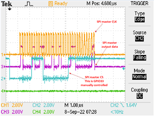
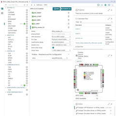
I'm using the F280045_56RSH uC to control an ADS1261 ADC. Due to routing issues, the normal SPIA CS can't being used. I'm using the "CUSTOM" setting in the "Use Case" for the SPIA master and GPIO33 pin 29 for the CS which is manually controlled. This is all configured in the .syscfg GUI. Please see syscfg GUIs, code and scope image below. I'm sending out 4 bytes of data, 2 bytes per CS cycle. The CS goes low as expected, please see scope capture below. However, I noticed two things. First, the 4 bytes are not separated with any time delay between them, they're contiguous. I would've thought there would be some time between each byte. Second, there are two CS is being generated but they're being overrun. Please help on these issues. Thank you.

//
// This function performs the basic ADC initialization.
//
void ADC_init(void)
{
    ADC_RST();
    //
    // Write the MODE0 register
    // Set the sample rate to 7200SPS and the filter to SINC3.
    // (MODE0_DR_7200_SPS | MODE0_SINC3) = 0x62
    //
    ADC_Write_Reg(REG_ADDR_MODE0, (MODE0_DR_7200_SPS | MODE0_SINC3));

    //
    // Write the MODE1 register
    // Set the conversion start delay to 50us, chop mode to off and convertion mode to continuous.
    // (MODE1_DELAY_50_uST | MODE1_CHOP_OFF | MODE1_CONVRT_CONTINUOUS) = 0x01
    //
    ADC_Write_Reg(REG_ADDR_MODE1, (MODE1_DELAY_50_uS | MODE1_CHOP_OFF | MODE1_CONVRT_CONTINUOUS));

    //
    // Write the MODE2 register
    // Enables AIN2 and AIN3 as outputs.
    // Connect AIN2 to GPIO0 and AIN3 to GPIO1
    // These IOs control the bridge excitation direction switches.
    // (MODE2_GPIOCON_AIN3_ENABLE_MASK | MODE2_GPIOCON_AIN2_ENABLE_MASK) = 0x30
    //
    ADC_Write_Reg(REG_ADDR_MODE2, (MODE2_GPIOCON_AIN3_ENABLE_MASK | MODE2_GPIOCON_AIN2_ENABLE_MASK));

    //
    // Write the MODE3 register
    // Set AIN3's output to high. AIN2's output is default low.
    // MODE3_GPIODAT_AIN3_DATA_MASK = 0x02
    //
    ADC_Write_Reg( REG_ADDR_MODE3, MODE3_GPIODAT_AIN3_DATA_MASK);

    //
    // Write the REF register
    // Enable the internal reference to enable the internal current source to be used.
    // NOTE: any time the REF register is changed, REF_REFENB_MASK must be ORed with the change
    // in order to maintain the IDAC1 current output.
    // (REF_REFENB_MASK | REF_RMUXP_AVDD | REF_RMUXN_AVSS) = 0x15
    //
    ADC_Write_Reg(REG_ADDR_REF, (REF_REFENB_MASK | REF_RMUXP_AVDD | REF_RMUXN_AVSS));

    //
    // Write the IMUX1 and IMUX2 registers
    // Select IDAC1 and IDAC2 to be connected to AINCOM.
    // (IMUX_IMUX2_NOCONNECT | IMUX_IMUX1_AINCOM) = 0xFA
    //
    ADC_Write_Reg(REG_ADDR_IMUX, (IMUX_IMUX2_AINCOM | IMUX_IMUX1_AINCOM));

    //
    // Write the IMAG register
    // Set IDAC1 output to 500uA and IDAC2 to 100uA
    // (IMAG_IMAG2_100_uA | IMAG_IMAG1_500_uA) = 0x24
    // NOTE: The excitation current is set to 600uA to ensure that the voltage
    // at the current output pin does not exceed the 3.9V limit for a maximum
    // bridge resistance of 6350 ohm @ 50°C.
    //
    ADC_Write_Reg(REG_ADDR_IMAG, (IMAG_IMAG2_100_uA | IMAG_IMAG1_500_uA));
}
//
// This function writes to the designated ADC register.
//
void ADC_Write_Reg(uint8_t reg_addr, uint8_t reg_data)
{
    uint16_t tempData;
    uint16_t shifted_RegAddr;
    uint16_t shifted_Data;

    shifted_RegAddr = ((OPCODE_WREG + reg_addr) << 8);          // OPCODE_WREG is defined as 0x40
    shifted_Data = reg_data << 8;

    tempData = SPI_readDataNonBlocking(SPIA_BASE);              // Empty the receive register.
    ADC_CS(LOW);                                                // Enable CS for the ADC.
    SPI_writeDataBlockingNonFIFO(SPIA_BASE, shifted_RegAddr);   // Send write command (0x40) to ADS1261.
    tempData = SPI_readDataNonBlocking(SPIA_BASE);              // Empty the receive register.
    SPI_writeDataBlockingNonFIFO(SPIA_BASE, shifted_Data);      // Send out the data to ADS1261.
    tempData = SPI_readDataNonBlocking(SPIA_BASE);              // Empty the receive register.
    ADC_CS(HIGH);                                               // Disable CS for the ADC.

}