Other Parts Discussed in Thread: UNIFLASH
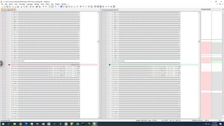
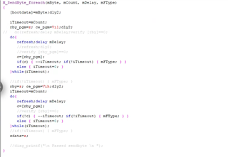
While programming 0x96550B5A to boot control register in DCSM OTP region under CPU1 it is failing after sending 0x96550B5A value to the chip. Will attach complete buffer value which we use to program the chip in the attachment below for OTP region of cpu1 data in the buffer it is arranged in big endian format and we send LSB first during programming using these pin to send data to the device K16 L17 N17 M16 M17 L16 J17 J16 pins and I will also attach a data pattern which works during program which does not throw failure. Only difference between those two data file is BOOT control region of OTP. Attached file contains left side which fails program right side which passes program. The highlighted it is the only changes between the file one which work and the one which fails program. Do we have to follow any other specific routine to program boot control bits??