This thread has been locked.

If you have a related question, please click the "Ask a related question" button in the top right corner. The newly created question will be automatically linked to this question.

TMS320F2808: TMS320F2808 Question

Part Number: TMS320F2808

The software code is like this:

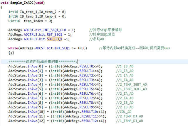
Software starts AD conversion, and then waits for SEQ1 sequence conversion completion flag INT_ SEQ1 to be set.  Under normal circumstances, wait about 6us after starting AD conversion, AD conversion will be completed, and corresponding INT_ SEQ1 will also be set. However, INT_SEQ1 occasionally appears in practical applications is always not set, and the program falls into a dead cycle. Has anyone ever encountered this situation? What is the general reason?

  • Wanhua,

    Perhaps there is some race condition with the setting of RST_SEQ1 and SOC_SEQ1 in back to back instructions(to be fair we don't have any requirements in the TRM that don't allow what the customer has done).

    Can customer place the INT_SEQ_CLR and RST_SEQ1 lines of code, after the read of the ADC Results has happened and see if that resolves things?  I'd like to get some separation between the that and the SOC_SEQ1 lines of code.

    Best,

    Matthew

  • 1、CAN the race condition between the setting of RST_SEQ1 and SOC_SEQ1 result the  dead cycle of AD?

    2、Is there any other reasons,like  Internal defect of DSP chip ? or Internal bonding wire delamination?

  • My theory is that the RST_SEQ1 has not fully propagated by the time the SOC_SEQ1 gets latched and causes the SOC_SEQ1 not to happen at all, so we get stuck since if SOC_SEQ1 never gets latched it will not happen again since we are waiting for the end of the conversion to happen(but it never started).

    Since this is not an ISR, is there any chance this function gets interrupted by an ISR from a different source?

    Right now I'm not suspecting defect or delam.  Does customer see this on multiple devices, or does only one device show this behavior?

    Best,

    Matthew

  • 1. I understand that according to the reason for the conflict of instructions you said, this problem should be easy to occur, but in practice, the probability of this problem is very low.

    2. This function is called within the Timer0 interrupt. The Timer0 interrupt is configured as non-interruptible, so this function will not be interrupted by other interrupt sources.

    3. Three of the nine devices have had this problem. After analyzing one of the chips with the problem, we found that the chip has a Bonding wire delamination problem。But I think the  Bonding wire delamination can not rasult this problem ,so can you give any other proposals?

    thank you very much.

  • Wanhua,

    I think it depends on which pin(s) have the delamination, especially if it is a power pin and we have reason to believe the device is not getting the correct supply voltage/current, this could lead to alot of different issues with code execution.  Or if the input clock pin had some issues and we start running out of specification wrt to the clock that could also give rise to issues.

    To be clear, I don't think my scenario should happen, but was something to try to rule out a timing issue. Those 3 instructions are all write instructions, so they will occur in the order written in the code, to my knowledge these are all single cycle execution events once they reach the ADC.

    Can customer try to run the device at a slower CPU clock than normal and see if this improves anything?  Or is it so low occurrence this is not practical?

    Best,

    Matthew