Hi,
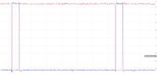
Im configuring an ePWM channel to trigger from the CMPSS module. I generate a TRIP signal that i compare with the DC module. The output of the DC module is later feed into the Action Qualifier module to trigger the ePWM. The issue is that after configuring the deadband module to generate a negated signal in the channel B, i get an overlap between channel A and B. Can someone help me with this issue?
I attach the section of code where i configure the EPWM channel.
//Time Base SubModule Register
(*ePWM[n]).TBCTL.bit.PRDLD = TB_IMMEDIATE; //Active Period Reg Load from Shadow Select // Set Immediate load
(*ePWM[n]).TBPRD = period;
(*ePWM[n]).TBPHS.bit.TBPHS = 0; // Time Base Phase High
(*ePWM[n]).TBCTR = 0; // Time Base Counter Register
(*ePWM[n]).TBCTL.bit.CTRMODE = TB_COUNT_UPDOWN;
(*ePWM[n]).TBCTL.bit.PHSEN = TB_DISABLE; // Counter Reg Load from Phase Reg Enable
//(*ePWM[n]).TBCTL.bit.SYNCOSEL = TB_CTR_CMPB; // Used to sync EPWM(n+1) "down-stream"
// SUbstitute
(*ePWM[n]).EPWMSYNCOUTEN.bit.CMPBEN = 1;
//
(*ePWM[n]).TBCTL.bit.HSPCLKDIV = TB_DIV1; // High Speed Time Base Clock Pre-Scale Bits
(*ePWM[n]).TBCTL.bit.CLKDIV = TB_DIV1; // Time Base Clock Pre-Scale Bits
// Counter compare submodule registers
(*ePWM[n]).CMPCTL.bit.SHDWAMODE = CC_IMMEDIATE; // Counter-compare A (CMPA) Register Operating Mode
(*ePWM[n]).CMPCTL.bit.SHDWBMODE = CC_IMMEDIATE; // Counter-compare B (CMPB) Register Operating Mode
(*ePWM[n]).CMPA.bit.CMPA = period-10000;
(*ePWM[n]).CMPB.bit.CMPB = period;
// Action Qualifier SubModule Registers
(*ePWM[n]).AQCTLA.bit.ZRO = AQ_CLEAR; // Action When TBCTR = 0
(*ePWM[n]).AQCTLA.bit.PRD = AQ_SET; //Action When TBCTR = TBPRD
// DeadBand Control Register
(*ePWM[n]).DBCTL.bit.OUT_MODE = DB_FULL_ENABLE;
(*ePWM[n]).DBCTL.bit.POLSEL = DB_ACTV_HIC; // Active Hi Complimentary
(*ePWM[n]).DBRED.bit.DBRED = 20; // Initial value
(*ePWM[n]).DBFED.bit.DBFED = 20; // Initial value
/////////////////////////////////////////////////////////////////////////////////////////////////////////////
// ePWM(n+1) init. EPWM(n+1) is the lagging leg /////////////////////////////////////////////////////////////////
n=0;
//Time Base SubModule Register
(*ePWM[n+1]).TBCTL.bit.PRDLD = TB_SHADOW;
(*ePWM[n+1]).TBPRD = period;
(*ePWM[n+1]).TBPHS.bit.TBPHS = 0; // Time Base Phase High
(*ePWM[n+1]).TBCTR = 0; // Time Base Counter Register
(*ePWM[n+1]).TBCTL.bit.CTRMODE = TB_COUNT_UPDOWN;
(*ePWM[n+1]).TBCTL.bit.PHSEN = TB_DISABLE; // Counter Reg Load from Phase Reg Enable
//(*ePWM[n+1]).TBCTL.bit.SYNCOSEL = TB_SYNC_IN; // Sync "flow through" mode
(*ePWM[n+1]).TBCTL.bit.HSPCLKDIV = TB_DIV1;
(*ePWM[n+1]).TBCTL.bit.CLKDIV = TB_DIV1;
//
(*ePWM[n+1]).EPWMSYNCINSEL.bit.SEL=0x01; // EPWMxSYNCIN Source Select Register -> EPWM1.SYNCOUT
//
// Counter compare submodule registers
(*ePWM[n+1]).CMPA.bit.CMPA = 200; // Initial value
(*ePWM[n+1]).CMPB.bit.CMPB = 100; // Initial value
(*ePWM[n+1]).CMPCTL.bit.LOADAMODE = CC_CTR_ZERO; // Active Counter-Compare A (CMPA) Load From Shadow Select Mode
(*ePWM[n+1]).CMPCTL.bit.SHDWAMODE = CC_SHADOW; // Counter-compare A (CMPA) Register Operating Mode
(*ePWM[n+1]).CMPCTL.bit.LOADBMODE = CC_CTR_ZERO;
(*ePWM[n+1]).CMPCTL.bit.SHDWBMODE = CC_SHADOW;
// Action Qualifier SubModule Registers
//(*ePWM[n+1]).AQCTLA.bit.CAU = AQ_SET; // Action When TBCTR = CMPA on Up Count
//(*ePWM[n+1]).AQCTLA.bit.CBD = AQ_CLEAR;
//(*ePWM[n+1]).AQCTLA.bit.ZRO = AQ_SET; // Action When TBCTR = 0
//(*ePWM[n+1]).AQCTLA.bit.PRD = AQ_CLEAR; //Action When TBCTR = TBPRD
// DeadBand Control Register
(*ePWM[n+1]).DBCTL.bit.OUT_MODE = DB_FULL_ENABLE;
(*ePWM[n+1]).DBCTL.bit.POLSEL = DB_ACTV_HIC; // Active Hi Complimentary
(*ePWM[n+1]).DBRED.bit.DBRED = 0; // Initial value
(*ePWM[n+1]).DBFED.bit.DBFED = 0; // Initial value
// Cycle-by-Cycle (CBC) Trip Zone for PWM n+1
// This section of code configures the DC (Digital Compare) module to trigger the PWM module using the TRIPIN4 signal.
// High state in TRIPIN4 shall trigger the PWM in a cycle by cycle bases.
EALLOW;
// DCACTL - Digital Compare A Control Register
(*ePWM[n+1]).DCACTL.bit.EVT1FRCSYNCSEL=1;
// DCTRIPSEL - Digital Compare Trip Select Register
(*ePWM[n+1]).DCTRIPSEL.bit.DCAHCOMPSEL = 0b0011; // Digital Compare A High Input Select Bits: 0011-> TRIPIN4
// TZDCSEL- Trip Zone Digital Comparator Select Register
(*ePWM[n+1]).TZDCSEL.bit.DCAEVT2 = 0b010; // Digital Compare Output A Event 2 Selection 010: DCAH = high, DCAL = don't care
// TZSEL- Trip Zone Select Register
//(*ePWM[n+1]).TZSEL.bit.DCAEVT2 = 1; // Digital Compare Output A Event 2 Select: 1-> Enable DCAEVT2 as a CBC trip source for this ePWM module
// TZCTL - Trip Zone Control Register
//(*ePWM[n+1]).TZCTL.bit.TZA=1;
// TZCTL2 - Trip Zone Control Register
//(*ePWM[n+1]).TZCTL2.bit.ETZE = 1; //1 ->Use trip action defined in TZCTL2, TZCTLDCA and TZCTLDCB. Settings in TZCTL are ignored
//(*ePWM[n+1]).TZCTL2.bit.TZAU = 0b111; //Trip Action On EPWMxA while Count direction is DOWN: 010-> Forced Lo (EPWMxA = Lo state)
//(*ePWM[n+1]).TZCTL2.bit.TZAD = 0b111; //Trip Action On EPWMxA while Count direction is DOWN: 010-> Forced Lo (EPWMxA = Lo state)
//(*ePWM[n+1]).TZCTL2.bit.TZBU = 0b111; //Trip Action On EPWMxB while Count direction is UP: 010-> Forced Lo (EPWMxB = Lo state)
//(*ePWM[n+1]).TZCTL2.bit.TZBD = 0b111; //Trip Action On EPWMxB while Count direction is UP: 010-> Forced Lo (EPWMxB = Lo state)
//(*ePWM[n+1]).TZCTLDCA.bit.DCAEVT1D = 0b111;
//(*ePWM[n+1]).TZCTLDCA.bit.DCAEVT1U = 0b111;
//(*ePWM[n+1]).TZCTLDCA.bit.DCAEVT2D = 0b111;
//(*ePWM[n+1]).TZCTLDCA.bit.DCAEVT2U = 0b111;
// Action Qualifier ////////////////////////////////////////////////////////////////////////////////////////////////
(*ePWM[n+1]).AQTSRCSEL.bit.T2SEL=0b0001; // Action Qualifier Trigger Event Source Select Register: 0001 -> DCAEVT2
//(*ePWM[n+1]).AQTSRCSEL.bit.T1SEL=0b0001; // Action Qualifier Trigger Event Source Select Register: 0001 -> DCAEVT2
(*ePWM[n+1]).AQCTLA2.bit.T2U=0b01; // Additional Action Qualifier Control Register For Output A: 01-> Clear: force EPWMxB output low
(*ePWM[n+1]).AQCTLA2.bit.T2D=0b10; // Additional Action Qualifier Control Register For Output A: 10-> Set: force EPWMxB output high
//(*ePWM[n+1]).AQCTLB2.bit.T2U=0b01; // Additional Action Qualifier Control Register For Output A: 01-> Clear: force EPWMxB output low
//(*ePWM[n+1]).AQCTLB2.bit.T2D=0b10; // Additional Action Qualifier Control Register For Output A: 10-> Set: force EPWMxB output high
//(*ePWM[n+1]).AQCTLB2.bit.T2D=0b11; // Additional Action Qualifier Control Register For Output B: 01-> Clear: force EPWMxB output low
// ePWM X-BAR Configuration ////////////////////////////////////////////////////////////////////////////////////////////////
// TRIP4MUX0TO15CFG - ePWM XBAR Mux Configuration for TRIP4
EPwmXbarRegs.TRIP4MUX0TO15CFG.bit.MUX0=0; // 00 -> Select .0 input for Mux0 ; 0.0 - CMPSS1.CTRIPH
// TRIP4MUXENABLE - ePWM XBAR Mux Enable for TRIP4
EPwmXbarRegs.TRIP4MUXENABLE.bit.MUX0=1; // 1-> Respective output of Mux0 is enabled to drive the TRIP4 of EPWM-XBAR
// TRIPOUTINV: ePWM XBAR Output Inversion Register
EPwmXbarRegs.TRIPOUTINV.bit.TRIP4=0; // 0: drives active high output 1: drives active-low output
EDIS;