This thread has been locked.

If you have a related question, please click the "Ask a related question" button in the top right corner. The newly created question will be automatically linked to this question.

TIDM-02000: Delays when Event Based Phase Shifting Operation in PSFB topology

Part Number: TIDM-02000
Other Parts Discussed in Thread: PMP23126, , C2000WARE, LAUNCHXL-F280049C

Hi,

I implemented the code for phase-shifted full bridge by using example code of TIDM-02000 and PMP23126. The phase shift between legs are generated by events for PCMC.

This is a benchtop test on demo-board F280049C. I provide external DC signal to CMPPS high input and I used ramp generator in order implement PCMC. 

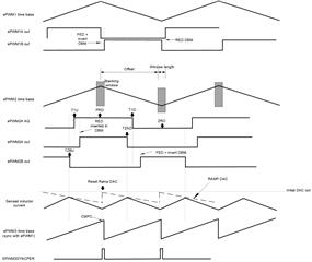
I generated 2xfrequency of ePWM8 in order generate SYNCPER signal in order sync. ePWMs and CMPSS. My main ePWMs are ePWM1,2. They are sync. to ePWM1.

(I use ePWM1,2,3,4 as PWM channels. All of them up-down count mode. ePWM5 and 6 -> SPI | ePWM7-> UART |  ePWM8 as boot pin configuration. Pins are connected to 3.3V with pull-up resistor.)

I could obtain %100 duty cycle without any problem. However, at %0 duty cycle there is delay between ePWM channels.

I generate %0 duty by providing lower reference value to CMPSS internal DAC. 

I generate %100 duty by providing higher reference value to CMPSS internal DAC.

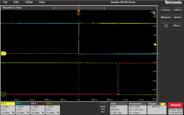
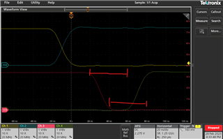
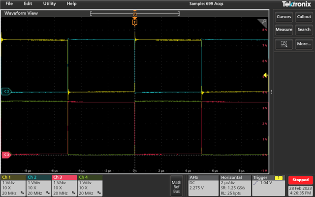
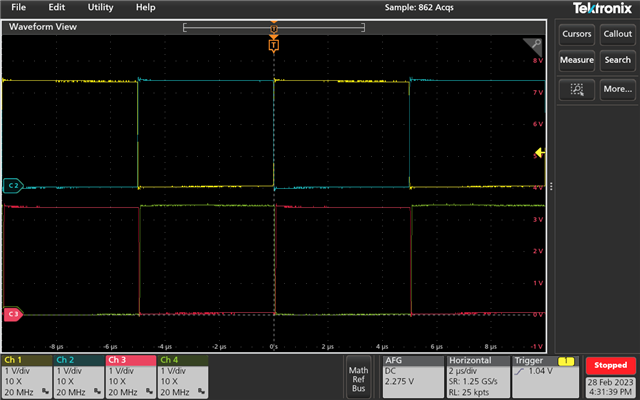
I inserted waveforms as below.  Yellow 1A, Blue 1B, Red 2A, Green 2B

%100 duty cycle case in PSFB topology. There is %100 match on Yellow and Green! Deadband is 0 for all channels in order to see performance. 

%0 duty cycle case in PSFB topology. There is %0 match on Yellow and Green! Deadband is 0 for all channels in order to see performance.

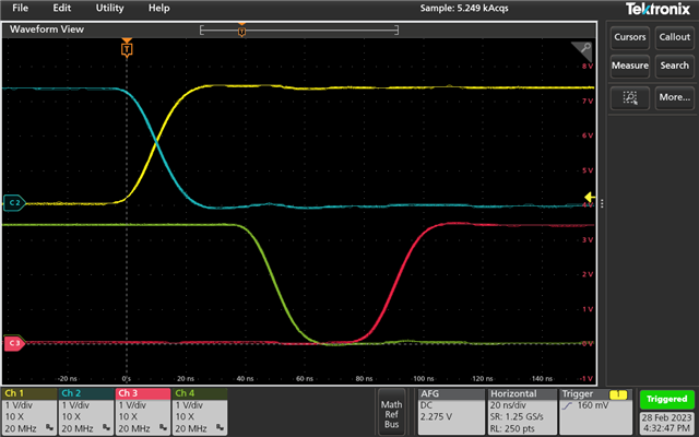
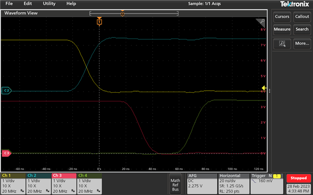
However, there is delay between rise and fall time between switches.

Details are as below.

1) Could you please explain how I could have %100 duty cycle and why not %0 duty cycle? What is the phenomenon behind?

As a remined, I don't use any filtering at CMPSS and I use blanking window at tripzone.

Sync. chain in ePWM timings might also be a problem... Blanking might be a problem....

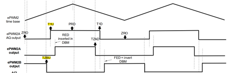
I have blanking at ePWM trip as below. I can provide more information if required.

    // Set the blanking window offset in TBCLK counts
    // An offset value in TBCLK counts is programmed
    // which determines at what point after the CTR = PRD or CTR = 0 pulse the blanking window starts.
    EPWM_setDigitalCompareWindowOffset(EPWM2_BASE, PeriodValue - 5);

    // Set the blanking window length in TBCLK counts
    // 10*TBLCK = 100nsec
    EPWM_setDigitalCompareWindowLength(EPWM2_BASE, 10);


  • Hi ,

    Thanks for the detailed info you provided. I am looking into this thread and will get back you in a few days.

    Regards,

    Chen

  • Hi, 

    I need help in order to continue. Could you please guide me?

  • Hi Gokhan,

    Sorry for the late response. For PWM1/2, are you using the same settings as below? 

    The delay you mentioned is actually between 1A/B and 2A/B in the last two pics, correct?

    And are you setting up an initial DAC value to be 0 to create the 0% duty cycle case? with slope compensation enabled? what is the slope?

    Regards,

    Chen

  • Hi Cheng,

    I use ePWM8 in order to generate SYNCPER signal.

    Sorry for the late response. For PWM1/2, are you using the same settings as below? 

    Very close configuration. Events are generated in ePWM2. Only difference is; I just use ePMW8 to set SYNCPER signal. It creates SYNCPER when TBCTR=PERIOD. And I added different blanking window as you can see above.

    And are you setting up an initial DAC value to be 0 to create the 0% duty cycle case? with slope compensation enabled? what is the slope?

    I set 0 to slope comp and 0 to DAC value. However, it isn't important. Because the delay between them also occurs when I have different duty cycles. I found it later. It seems that the delay comes from DC Submodule - Deadband Module or event generation based problems etc. You can see as below.

    all deadbands are loaded as 0.

    SYNCInit Configuration

    void SYNC_init(void)
    {
        SysCtl_setSyncOutputConfig(SYSCTL_SYNC_OUT_SRC_EPWM1SYNCOUT);
        //
        // For EPWM1, the sync input is: SYSCTL_SYNC_IN_SRC_EXTSYNCIN1
        //
        SysCtl_setSyncInputConfig(SYSCTL_SYNC_IN_EPWM4, SYSCTL_SYNC_IN_SRC_EPWM1SYNCOUT);
        SysCtl_setSyncInputConfig(SYSCTL_SYNC_IN_EPWM7, SYSCTL_SYNC_IN_SRC_EPWM1SYNCOUT);
    
    }

    ePWM1 Configuration

        EPWM_setPeriodLoadMode(EPWM1_BASE, EPWM_PERIOD_SHADOW_LOAD);
    
        // Time-Base Submodule Configurations
        EPWM_setClockPrescaler(EPWM1_BASE,EPWM_CLOCK_DIVIDER_1,EPWM_HSCLOCK_DIVIDER_1);
        EPWM_setTimeBasePeriod(EPWM1_BASE, PeriodValue);
        EPWM_setTimeBaseCounter(EPWM1_BASE, 0U);
        EPWM_setTimeBaseCounterMode(EPWM1_BASE, EPWM_COUNTER_MODE_UP_DOWN);
    
        //
        // Phase Configuration and Set
        // Configure PWM base1 as master
        // SetPhaseShift as zero!
        //
        EPWM_disablePhaseShiftLoad(EPWM1_BASE);
        EPWM_setPhaseShift(EPWM1_BASE, 0U);
        EPWM_setSyncOutPulseMode(EPWM1_BASE, EPWM_SYNC_OUT_PULSE_ON_COUNTER_ZERO);

    ePWM2 Configuration

    I change deadband later on through UART. I set it 0.

        // MISC. Period Load Mode
        EPWM_setPeriodLoadMode(EPWM2_BASE, EPWM_PERIOD_SHADOW_LOAD);
    
        // Time-Base Submodule Configurations
        EPWM_setClockPrescaler(EPWM2_BASE,EPWM_CLOCK_DIVIDER_1,EPWM_HSCLOCK_DIVIDER_1);
        EPWM_setTimeBasePeriod(EPWM2_BASE, PeriodValue);
        EPWM_setTimeBaseCounter(EPWM2_BASE, 0U);
        EPWM_setTimeBaseCounterMode(EPWM2_BASE, EPWM_COUNTER_MODE_UP_DOWN);
    
        //
        // Phase Configuration and Set
        // Configure PWM base2 as slave
        // SetPhaseShift = Value*TBCLK = Value*10nsec
        //
        EPWM_enablePhaseShiftLoad(EPWM2_BASE);
        EPWM_setSyncOutPulseMode(EPWM2_BASE, EPWM_SYNC_OUT_PULSE_ON_EPWMxSYNCIN);
    
        EPWM_setPhaseShift(EPWM2_BASE, 2); // Value*TBCLKs Phase-Shift is Set
        EPWM_setCountModeAfterSync(EPWM2_BASE, EPWM_COUNT_MODE_UP_AFTER_SYNC);
    
        // Counter-Compare Submodule Configurations
        EPWM_setCounterCompareShadowLoadMode(EPWM2_BASE,EPWM_COUNTER_COMPARE_A,EPWM_COMP_LOAD_ON_CNTR_ZERO);
        EPWM_setCounterCompareShadowLoadMode(EPWM2_BASE,EPWM_COUNTER_COMPARE_B,EPWM_COMP_LOAD_ON_CNTR_ZERO);
    
        EPWM_setCounterCompareValue(EPWM2_BASE, EPWM_COUNTER_COMPARE_A, 0);
        EPWM_setCounterCompareValue(EPWM2_BASE, EPWM_COUNTER_COMPARE_B, 0);
    
        //
        // to start don't configure the PWM to do anything
        //
        HWREGH(EPWM2_BASE + EPWM_O_AQCTLA) = 0;
    
        // Action-Qualifier Submodule Configurations
        // ePWM2A Actions
        // CTR = ZERO , set to 0
        // CTR = PRD , set to 1
        // CTR = T1U , set to 1
        // CTR = T1D , set to 0
        //
        EPWM_setActionQualifierAction(EPWM2_BASE,EPWM_AQ_OUTPUT_A,EPWM_AQ_OUTPUT_LOW,EPWM_AQ_OUTPUT_ON_TIMEBASE_ZERO);
        EPWM_setActionQualifierAction(EPWM2_BASE,EPWM_AQ_OUTPUT_A,EPWM_AQ_OUTPUT_HIGH,EPWM_AQ_OUTPUT_ON_TIMEBASE_PERIOD);
        EPWM_setActionQualifierAction(EPWM2_BASE,EPWM_AQ_OUTPUT_A,EPWM_AQ_OUTPUT_NO_CHANGE,EPWM_AQ_OUTPUT_ON_TIMEBASE_UP_CMPA);
        EPWM_setActionQualifierAction(EPWM2_BASE,EPWM_AQ_OUTPUT_A,EPWM_AQ_OUTPUT_NO_CHANGE,EPWM_AQ_OUTPUT_ON_TIMEBASE_DOWN_CMPA);
        EPWM_setActionQualifierAction(EPWM2_BASE,EPWM_AQ_OUTPUT_A,EPWM_AQ_OUTPUT_NO_CHANGE,EPWM_AQ_OUTPUT_ON_TIMEBASE_UP_CMPB);
        EPWM_setActionQualifierAction(EPWM2_BASE,EPWM_AQ_OUTPUT_A,EPWM_AQ_OUTPUT_NO_CHANGE,EPWM_AQ_OUTPUT_ON_TIMEBASE_DOWN_CMPB);
        EPWM_setActionQualifierAction(EPWM2_BASE,EPWM_AQ_OUTPUT_A,EPWM_AQ_OUTPUT_HIGH, EPWM_AQ_OUTPUT_ON_T1_COUNT_UP);
        EPWM_setActionQualifierAction(EPWM2_BASE,EPWM_AQ_OUTPUT_A,EPWM_AQ_OUTPUT_LOW, EPWM_AQ_OUTPUT_ON_T1_COUNT_DOWN);
    
        // Action-Qualifier Submodule Configurations
        // ePWM2B Actions
        // CTR = ZERO , set to 0
        // CTR = PRD , set to 1
        // CTR = T1U , set to 1
        // CTR = T1D , set to 0
        //
        EPWM_setActionQualifierAction(EPWM2_BASE,EPWM_AQ_OUTPUT_B,EPWM_AQ_OUTPUT_LOW,EPWM_AQ_OUTPUT_ON_TIMEBASE_ZERO);
        EPWM_setActionQualifierAction(EPWM2_BASE,EPWM_AQ_OUTPUT_B,EPWM_AQ_OUTPUT_HIGH,EPWM_AQ_OUTPUT_ON_TIMEBASE_PERIOD);
        EPWM_setActionQualifierAction(EPWM2_BASE,EPWM_AQ_OUTPUT_B,EPWM_AQ_OUTPUT_NO_CHANGE,EPWM_AQ_OUTPUT_ON_TIMEBASE_UP_CMPA);
        EPWM_setActionQualifierAction(EPWM2_BASE,EPWM_AQ_OUTPUT_B,EPWM_AQ_OUTPUT_NO_CHANGE,EPWM_AQ_OUTPUT_ON_TIMEBASE_DOWN_CMPA);
        EPWM_setActionQualifierAction(EPWM2_BASE,EPWM_AQ_OUTPUT_B,EPWM_AQ_OUTPUT_NO_CHANGE,EPWM_AQ_OUTPUT_ON_TIMEBASE_UP_CMPB);
        EPWM_setActionQualifierAction(EPWM2_BASE,EPWM_AQ_OUTPUT_B,EPWM_AQ_OUTPUT_NO_CHANGE,EPWM_AQ_OUTPUT_ON_TIMEBASE_DOWN_CMPB);
        EPWM_setActionQualifierAction(EPWM2_BASE,EPWM_AQ_OUTPUT_B,EPWM_AQ_OUTPUT_HIGH, EPWM_AQ_OUTPUT_ON_T1_COUNT_UP);
        EPWM_setActionQualifierAction(EPWM2_BASE,EPWM_AQ_OUTPUT_B,EPWM_AQ_OUTPUT_LOW, EPWM_AQ_OUTPUT_ON_T1_COUNT_DOWN);
    
        //
        // Set DCEVTFILT as the trigger source for Channel A
        //
        EPWM_setActionQualifierT1TriggerSource(EPWM2_BASE,
                                        EPWM_AQ_TRIGGER_EVENT_TRIG_DC_EVTFILT);
    
        // Digital Compare and Comparator-X-Bar Configuration
        // Disable all the muxes first
        XBAR_enableEPWMMux(XBAR_TRIP4, 0x00);
    
        //
        // Setup PWM TRIP 4 as the destination for CMPSS5H output (PCMC)
        // TRIP4 will be ACTIVE if CTRIPH is HIGH at CMPSS5
        XBAR_setEPWMMuxConfig(XBAR_TRIP4, XBAR_EPWM_MUX08_CMPSS5_CTRIPH);
        XBAR_enableEPWMMux(XBAR_TRIP4, XBAR_MUX08);
    
        //
        // DCAH = TRIP5 = Comparator 1H output
        //
        EPWM_selectDigitalCompareTripInput(EPWM2_BASE, EPWM_DC_TRIP_TRIPIN4,
                                            EPWM_DC_TYPE_DCAH);
    
        // DCAH = high
        EPWM_setTripZoneDigitalCompareEventCondition(EPWM2_BASE, EPWM_TZ_DC_OUTPUT_A2,
                                            EPWM_TZ_EVENT_DCXH_HIGH);
    
        // Set the source for digital compare filter as DCAEVT2
        EPWM_setDigitalCompareEventSource(EPWM2_BASE, EPWM_DC_MODULE_A,EPWM_DC_EVENT_2,
                                          EPWM_DC_EVENT_SOURCE_FILT_SIGNAL);
    
        // Allow ASYNC DCAEVT2 for trip zone actions
        EPWM_setDigitalCompareEventSyncMode(EPWM2_BASE, EPWM_DC_MODULE_A,
                                            EPWM_DC_EVENT_2,
                                            EPWM_DC_EVENT_INPUT_NOT_SYNCED);
    
        // Select DCAEVT2 cycle by cycle trip
        EPWM_enableTripZoneSignals(EPWM2_BASE, EPWM_TZ_SIGNAL_DCAEVT2);
    
        // Event Filtering Configuration (inside digital compare)
        // Enable DC filter blanking window
        EPWM_enableDigitalCompareBlankingWindow(EPWM2_BASE);
        //EPWM_disableDigitalCompareBlankingWindow(EPWM2_BASE);
    
        // Set the signal source that will be filtered.
        EPWM_setDigitalCompareFilterInput(EPWM2_BASE, EPWM_DC_WINDOW_SOURCE_DCAEVT2);
    
        // Set the Digital Compare filter blanking pulse.
        EPWM_setDigitalCompareBlankingEvent(EPWM2_BASE,
                                         EPWM_DC_WINDOW_START_TBCTR_ZERO_PERIOD);
    
        // Set the blanking window offset in TBCLK counts
        // An offset value in TBCLK counts is programmed
        // which determines at what point after the CTR = PRD or CTR = 0 pulse the blanking window starts.
        EPWM_setDigitalCompareWindowOffset(EPWM2_BASE, PeriodValue - 100);
    
        // Set the blanking window length in TBCLK counts
        // 10*TBLCK = 100nsec
        EPWM_setDigitalCompareWindowLength(EPWM2_BASE, 200);
    
        //
        // Trip-zone event actions
        // What do we want the CBC events to do?
        // TZAx events can force EPWMxA
        // TZBx events can force EPWMxB
        //
        EPWM_setTripZoneAdvAction(EPWM2_BASE, EPWM_TZ_ADV_ACTION_EVENT_TZA_D,
                                  EPWM_TZ_ADV_ACTION_LOW);
        EPWM_setTripZoneAdvAction(EPWM2_BASE, EPWM_TZ_ADV_ACTION_EVENT_TZA_U,
                                  EPWM_TZ_ADV_ACTION_DISABLE);
        EPWM_setTripZoneAdvAction(EPWM2_BASE, EPWM_TZ_ADV_ACTION_EVENT_TZB_U,
                                  EPWM_TZ_ADV_ACTION_LOW);
        EPWM_setTripZoneAdvAction(EPWM2_BASE, EPWM_TZ_ADV_ACTION_EVENT_TZB_D,
                                  EPWM_TZ_ADV_ACTION_DISABLE);
        EPWM_setTripZoneAction(EPWM2_BASE, EPWM_TZ_ACTION_EVENT_TZA,
                               EPWM_TZ_ACTION_DISABLE);
        EPWM_setTripZoneAction(EPWM2_BASE, EPWM_TZ_ACTION_EVENT_TZB,
                               EPWM_TZ_ACTION_DISABLE);
    
        //
        // Select CBC clear event
        EPWM_selectCycleByCycleTripZoneClearEvent(EPWM2_BASE,
                               EPWM_TZ_CBC_PULSE_CLR_CNTR_ZERO_PERIOD);
    
        //
        // Clear any spurious trip
        EPWM_clearTripZoneFlag(EPWM1_BASE, (EPWM_TZ_INTERRUPT_OST |
                EPWM_TZ_INTERRUPT_DCAEVT2 | EPWM_TZ_SIGNAL_DCBEVT1));
        EPWM_clearTripZoneFlag(EPWM2_BASE, (EPWM_TZ_INTERRUPT_OST |
                EPWM_TZ_INTERRUPT_DCAEVT2 | EPWM_TZ_SIGNAL_DCBEVT1));
    
    
        // Dead band counter runs at TBCLK rate
        EPWM_setDeadBandCounterClock(EPWM2_BASE, EPWM_DB_COUNTER_CLOCK_FULL_CYCLE);
    
        // Set the RED and FED values : (Value*10ns)
        EPWM_setRisingEdgeDelayCount(EPWM2_BASE, 15);
        EPWM_setFallingEdgeDelayCount(EPWM2_BASE, 15);
    
        //DelayMode select
        //EPWM_DB_RED   - Rising Edge delay,
        //EPWM_DB_FED   - Falling Edge delay
        //true     - Falling edge or Rising edge delay is applied.
        //false    - Dead Band delay is bypassed.
        EPWM_setDeadBandDelayMode(EPWM2_BASE, EPWM_DB_RED, true);
        EPWM_setDeadBandDelayMode(EPWM2_BASE, EPWM_DB_FED, true);
        EPWM_setRisingEdgeDeadBandDelayInput(EPWM2_BASE, EPWM_DB_INPUT_EPWMA);
        EPWM_setFallingEdgeDeadBandDelayInput(EPWM2_BASE, EPWM_DB_INPUT_EPWMB);
    
        // xA is RED, same!!!
        EPWM_setDeadBandDelayPolarity(EPWM2_BASE, EPWM_DB_RED, EPWM_DB_POLARITY_ACTIVE_HIGH);
    
        // xB is FED, inverted (AHC) !!!
        EPWM_setDeadBandDelayPolarity(EPWM2_BASE, EPWM_DB_FED, EPWM_DB_POLARITY_ACTIVE_LOW);
    
        // Do Not Switch Output A with Output B (No Swapping!)
        EPWM_setDeadBandOutputSwapMode(EPWM2_BASE, EPWM_DB_OUTPUT_A, false);                        // DO NOT Switch Output A with Output B
        EPWM_setDeadBandOutputSwapMode(EPWM2_BASE, EPWM_DB_OUTPUT_B, false);
    

    ePWM8 Configuration

        EALLOW;
        EPWM_setPeriodLoadMode(EPWM8_BASE, EPWM_PERIOD_SHADOW_LOAD);
    
        // Time-Base Submodule Configurations
        EPWM_setClockPrescaler(EPWM8_BASE,EPWM_CLOCK_DIVIDER_1,EPWM_HSCLOCK_DIVIDER_1);
        EPWM_setTimeBasePeriod(EPWM8_BASE, PeriodValue-1);
        EPWM_setTimeBaseCounter(EPWM8_BASE, 0);
        EPWM_setTimeBaseCounterMode(EPWM8_BASE, EPWM_COUNTER_MODE_UP);
    
        //
        // Phase Configuration and Set
        // Configure PWM base3 as slave
        // SetPhaseShift = Value*TBCLK = Value*10nsec
        EPWM_enablePhaseShiftLoad(EPWM8_BASE);
        EPWM_setPhaseShift(EPWM8_BASE, 2); // Will be clarified later on!
        EPWM_setSyncOutPulseMode(EPWM8_BASE, EPWM_SYNC_OUT_PULSE_ON_EPWMxSYNCIN);
        EPWM_setCountModeAfterSync(EPWM8_BASE, EPWM_COUNT_MODE_UP_AFTER_SYNC);
    
        //
        // Counter-Compare Submodule Configurations
        EPWM_setCounterCompareShadowLoadMode(EPWM8_BASE,EPWM_COUNTER_COMPARE_A,EPWM_COMP_LOAD_ON_CNTR_ZERO);
        EPWM_setCounterCompareShadowLoadMode(EPWM8_BASE,EPWM_COUNTER_COMPARE_B,EPWM_COMP_LOAD_ON_CNTR_ZERO);
    
    
        EPWM_setCounterCompareValue(EPWM8_BASE, EPWM_COUNTER_COMPARE_A, 0);
        EPWM_setCounterCompareValue(EPWM8_BASE, EPWM_COUNTER_COMPARE_B, 0);
    
        HRPWM_setSyncPulseSource(EPWM8_BASE,HRPWM_PWMSYNC_SOURCE_PERIOD);
    
        EDIS;

    CMPSS Configuration

        CMPSS_configHighComparator(CMPSS5_BASE,
                                   CMPSS_INSRC_DAC)
                                   
        ASysCtl_selectCMPHPMux(ASYSCTL_CMPHPMUX_SELECT_5,
                               0);
                               
        CMPSS_configDAC(CMPSS5_BASE, CMPSS_DACREF_VDDA |
                        CMPSS_DACVAL_PWMSYNC | CMPSS_DACSRC_RAMP);
        
        CMPSS_configRamp(CMPSS5_BASE,0,0,0U,8U,true);
        CMPSS_initFilterHigh(CMPSS5_BASE);
            //
        // Configure the output signals. Both CTRIPH and CTRIPOUTH will be fed by
        // the asynchronous comparator output.
        //
        CMPSS_configOutputsHigh(CMPSS5_BASE,
                                CMPSS_TRIP_ASYNC_COMP | CMPSS_TRIPOUT_ASYNC_COMP);
    
        // Clear the latched comparator events
        CMPSS_clearFilterLatchHigh(CMPSS5_BASE);
        CMPSS_clearFilterLatchLow(CMPSS5_BASE);
    
        // Enables the CMPSS module.
        CMPSS_enableModule(CMPSS5_BASE);
        DEVICE_DELAY_US(500);

  • Hello Gokhan,

    I'll take a look at your queries in detail, however, before going down that path too far, can you clarify why you are using the TIDM-2000 firmware on the PMP23126 hardware? The PMP23126 hardware already includes its own firmware which also implements a PCMC phase-shifted full-bridge DC/DC converter. You can find the design guide and reference firmware at in the C2000 digital power SDK. The firmware is also based on the F280049C.

    https://www.ti.com/tool/C2000WARE-DIGITALPOWER-SDK

    C:\ti\c2000\C2000Ware_DigitalPower_SDK_4_02_00_00\solutions\pmp23126

  • Looking in detail over your question, per my understanding your main question on PWM2A and PWM2B. Specifically, why there is a delay between the two outputs. Is this correct? 

    If you notice in the configuration for PMP23126 (same PSFB config as TIDM-2000), there is a slight difference of when PWM2A output is set high vs when the PWM2B output is set low. The PWM2A high state is driven from the action qualifier (T1U), while the PWM2B low state is driven from the trip zone (TZBU). The trip zone is faster than the action qualifier and it is this difference what you are seeing on the scope. Similar logic applies to the difference between PWM2A low state and PWM2B high state.

    Note that you don't see this on PWM1A/B because in that case, PWM1B is simply an inverted version of PWM1A. This is called the complementary configuration in the documentation.

  • Hello Gus,

    Thank you for your help. I investigated both software, because I will implement PCMC on my board. Therefore, I checked all the software option. Both have PCMC implementation and question would be same. I chose TIDM-02000. I obtained above waveforms from LAUNCHXL-F280049C. I externally provided DC signal to ADC port.

  • Hi Gus,

    Thank you for detailed investigation and help.

    Looking in detail over your question, per my understanding your main question on PWM2A and PWM2B. Specifically, why there is a delay between the two outputs. Is this correct?

    Yes, you are correct. The turn-on of PWM2A and turn-off PWM2B has delay and vice versa although I wrote 0 to RED and FED values.

    The PWM2A high state is driven from the action qualifier (T1U), while the PWM2B low state is driven from the trip zone (TZBU). The trip zone is faster than the action qualifier and it is this difference what you are seeing on the scope. Similar logic applies to the difference between PWM2A low state and PWM2B high state.

    Yes, I got the point. Just one event T1 drives PWM2B low and PWM2A to high, but there is 60nsec delay during driving high. Is 60nsec expected correct value?

    I also couldn't understand how %100 duty is achieved. Because I have blanking window and when PWM2B and PWM1A matches %100; TZAB is generated at blanking window duration. However, blanking window effect my minimum duty.

    Thank you in advance.

  • By the way, if I use PCMC to obtain transformer balance in volt.usec, I generate 60nsec delay between legs in my hand at PWM module. It seemed me not a good solution. Can you comment on it?

  • Yes, I got the point. Just one event T1 drives PWM2B low and PWM2A to high, but there is 60nsec delay during driving high. Is 60nsec expected correct value?

    There is this note in the PWM chapter of the TRM:

    The TZn signals, when used as a DCEVT tripping functions, are treated as a normal input signal and can be defined to be active-high or active-low inputs. ePWM outputs are asynchronously tripped when either the TZn, DCAEVTx.force, or DCBEVTx.force signals are active. For the condition to remain latched, a minimum of 3*TBCLK sync pulse width is required. If pulse width is < 3*TBCLK sync pulse width, the trip condition can or can not get latched by CBC or OST latches.

    That would lead me to believe that there should be a difference of at least 3 TBCLK cycles. A difference of 60ns would make sense if your TBCLK was configured for 50MHz. However, in your description and code snippets, it seems like TBCLK is configured for 100MHz.Can you clarify what is your TBCLK configuration?

    I also couldn't understand how %100 duty is achieved. Because I have blanking window and when PWM2B and PWM1A matches %100; TZAB is generated at blanking window duration. However, blanking window effect my minimum duty.

    I suspect this is why the PWMs configurations also use PRD and ZRO as action events. In other words, if your CMPSS event happens during the blanking period, the PRD and ZRO will still set/clear the PWM outputs.

  • By the way, if I use PCMC to obtain transformer balance in volt.usec, I generate 60nsec delay between legs in my hand at PWM module. It seemed me not a good solution. Can you comment on it?

    I am sorry, I do not understand the question.

  • Hi Gus,

    Thank you for answers.

    That would lead me to believe that there should be a difference of at least 3 TBCLK cycles. A difference of 60ns would make sense if your TBCLK was configured for 50MHz. However, in your description and code snippets, it seems like TBCLK is configured for 100MHz.Can you clarify what is your TBCLK configuration?

    Yes, my TBCLK is 100Mhz.

    I suspect this is why the PWMs configurations also use PRD and ZRO as action events. In other words, if your CMPSS event happens during the blanking period, the PRD and ZRO will still set/clear the PWM outputs.

    Yes, I got the point.

    By the way, if I use PCMC to obtain transformer balance in volt.usec, I generate 60nsec delay between legs in my hand at PWM module.

    In here, I mean that PCMC in PSFB is also used to set flux balance for power transformer. However, at PCMC software implementation, I inherently have 60nsec delay (between 2A and 2B) in power drives because of event based PWM tripping. That means during PCMC implementation and having benefits of PCMC, 60nsec delay occurs inside of MCU. It may lead to mismatch drives of power switches. I wondered your comments on it. 

  • At a PWM switching frequency of 100kHz, that 60ns is 0.6% of the switching period. It is small enough that it should not have an effect on the balance of the transformer. Note that the primary side switches themselves may take longer to actually switch their outputs as well. For the PMP23126 3kW design, this has not been an issue. 

  • Thank you Gus,

    Just one open issue, is the 60nsec delay between 2A and 2B is normal considering my TBCLK is 100Mhz?

  • Looking at your scope waveforms more closely, I believe it is not accurate to say the 2A and 2B edges are 60ns apart. You have to measure start of transition for both signals or end of transition for both signals, not mix and match. In this case, the difference is ~40ns. The extra 10ns is likely the CMPSS signal getting aligned to the internal SYSCLK of the device (10ns clock edge). 

  • Thank you Gus, you helped so much.