Because of the Thanksgiving holiday in the U.S., TI E2E™ design support forum responses may be delayed from November 25 through December 2. Thank you for your patience.

This thread has been locked.

If you have a related question, please click the "Ask a related question" button in the top right corner. The newly created question will be automatically linked to this question.

TMS320F280025: Control the stepper motor but have a jitter

Part Number: TMS320F280025

Hi Team,

Customer use 64pin F280025 to control a stepper. Customer sample the shunt resistor with the ADC in MCU.

But they found the motor will jitter,when EFT test(2000V, 5kHz/100kHz, 75 pulse each 300ms). We watch the waveform in oscilloscope. 
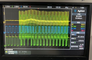
we found phase current is not very smooth(the yellow), and the PWM duty cycle is change(the green). AI pin for ADC might over 3.6V during the EFT test.

Customer use the software reference to control the PWM, the motor won't jitter.

If make a filter to delete the outliers form AD sampling, there will be over-current in their board.

Without EFT test, the motor preform well. And customer also use 80pin F280025 in another product, there is no that problem in EFT test.
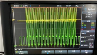
Add some TVS isn't change the result, and add GPIO filtter in software  also not change the result.

And we test other customer's product(stepper contorl by 280025) there is also the same probem. 

But in customer last platform 28034, there is also no problem. The 280025 and 28034 is almost the same design.

Do you have any idea to solve the problem?

Thanks alot.

  • Minghao,

    Q1)When we say that F28034 based design didn't have any issue, do we know if there is still pin noise/coupling voltage on the sampled ADC pin?

    Q2)In the current design is there noise physically coupled to the ADC input channel being sampled, or do we believe that other ADC pin has noise/overvoltage event on it and this is causing bad reading on the ADC channel that is being sampled.

    Q3)Can you clarify that the EFT test, this is radiated noise near the device?

    Q4)s customer using internal ADC reference or external ADC reference(voltage on VREFHI from external source)?

    Q5)Also, if you could give ADC channel usage, i.e. which ADC channel has the issue from above, as well as what the connections are for the rest of the ADC channels it will help.

    Q6)Has customer tried to change the sample trigger to see if they can avoid the noise?

    Best,

    Matthew

  • Q1-They make a test found that all the situation has the same interference. They say the design almost the same in those platform.

    Q2-There are some interference propagation path. The voltage for the two side of the shunt resistor, the power for the MCU, os the PCB layout.

    Q3-Customer add a interference in the board power input to finish FFT test. The interference is two types, one is 2000V 5KHz continue 75 cycle. The other is 2000V 100KHz continue 75 cycle. They add some protect device, such as some TVS between power and ground, and double-sided TVS between AO pin and GND.   

    Q4-The reference voltage is come from outside.

    Q5-18\19\20\13pin.

    Q6-How to change the sample trigger? Customer add a digital low pass filter to ADC, Which means they throw away the noise sampling point in MCU. But in that situation,  

  • Minghao,

    Could customer change to internal reference temporarily to see if this changes anything?  They would need to remove R77 on the PCB as well for this experiment.

    I'd like to understand if the noise is getting coupled on the ADC input itself, or if the VREFHI voltage is getting noise coupling.  Internal ref would at least rule that out.

    Best,

    Matthew

  • Customer has test this situation, if they use internal reference with R77 on the PCB, they could pass the test. In this situation the noise still could sampling by ADC, but MCU not use it as a reference.

  • I misunderstand you reply in the past.

    I have adviced customer to test changing the ADC reference voltage source.

  • Customer says there isn't any improve after changing the ADC reference voltage source.

  • Minghao,

    Please give me another day to respond back.

    Best,

    Matthew

  • Minghao,

    While the same configuration on the F28034 is not seeing this issue, the ADCs on these 2 devices are different so there could be some different coupling effecting going on.

    I'm going to preface the below with the statement that violating the DS limits on pin voltages (>VDDA) can cause issues.  https://www.ti.com/document-viewer/TMS320F280025C/datasheet/GUID-XXXXXXXX-SF0T-XXXX-XXXX-000000067422#GUID-XXXXXXXX-SF0L-XXXX-XXXX-000000067422

    Do we know if customer sees this sampled noise on all the pins or just some pins?  Since this is due to some emissions from a nearby source, I suppose we need to consider that this is coming on all the pins at the same time. 

    Perhaps something the customer could try, if they could reduce the power of the emission source, such that they do not see above VDDA and see if the issue goes away, that would at least confirm this is the cause.  In terms of limiting the effect we may have to look to add some blocking filters to some of the pins, or we could increase the S/H time to see if we can average the noise out.

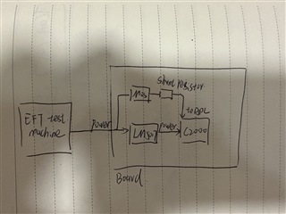
    Finally, could you describe the test setup, i.e. how is the ETF intended to effect the system?  Is this through radiated emissions near the device; or injected onto the board? 

    Best,
    Matthew

  • The noise is added in the power input for the all board. So it could seen form almost all the input pins at the same time.

    The picture is how the test influence C2000.

  • One thing to check is if there is voltage above VDDA applied to a ADC channel that shares a CMPSS mux with other channels it can reverse bias the mux switch and force turn on that path.  This would, in effect, short that signal to the other signals on that mux and then show up in the ADC sample.  Can customer check to see if this dependence is what is showing up in their system?

    Best,

    Matthew