This thread has been locked.

If you have a related question, please click the "Ask a related question" button in the top right corner. The newly created question will be automatically linked to this question.

Configuration to measure voltages of batteries in series with F28377S

Other Parts Discussed in Thread: INA143, INA333

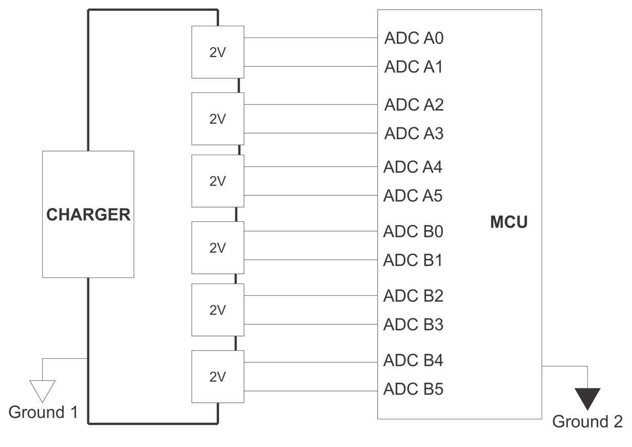
I'm implementing a battery voltage monitoring system which uses the MCU ADC differential mode like the picture below. The batteries are connected in series and I'm quite sure that battery ground and MCU ground are isolated. The MCU is the F28377S from Texas Instrument, it's a 3.3V MCU, it has 16 single ended ADC channels that could be paired up into 8 differential channels.

With this configuration, I hope that there will be no ground connection between the charger and and the MCU. With the ground completely isolated, no common mode DC offset, the MCU will be able to handle a 12V battery pack since its ADC only tolerates up to 3V.

  • Hi,

    Are you confirming your connections or informing the community on how its done :) ?
    If the former, you're connections are correct and yes grounds seem to be very well isolated.

    Regards,
    Gautam
  • I'm here to confirm the idea, Gautam :). Blowing up 39$ is not a good experience to have.

    What I know about the differential mode on the F28377S ADC is that it uses the results of 2 adjacent channels and take the difference between the two. However, let's set aside the fact that the MCU will be probably burned, if one channel is 6V and the other is 8V, ADC results will be capped at 3V and the result will be zero, right?

  • I think it's not a good idea to detect battery voltage like this because  MCU can't stand so high common mode voltage.

    I think signal condition circuit is necessary.

    you can check dataheet of INA143 or INA333.

  • Hac Le said:
    let's set aside the fact that the MCU will be probably burned, if one channel is 6V and the other is 8V, ADC results will be capped at 3V and the result will be zero, right?

    If you've a clamping diode it will be clamped at 3V or else the channel will get damaged. But this case should not occur, right?

  • That's why I'm asking for you guys' comments. I don't know whether the common mode DC offset would occur or not.
  • Hi Hac Le,

    This is definitely not going to work without signal conditioning circuitry, both from a functional perspective, and because the device will be destroyed in this configuration.

    Functionally, the differential inputs need a common mode voltage of VREFHI/2.  The allowance on this is +/-50mV.  This means that relative to VSSA/VREFLO, the average of the positive and negative ADC input pair needs to be roughly VREFHI/2.  As one input increases, the other should decrease to maintain the same common mode.  If you have a fully differential op-amp with a wide input common mode range and the output common mode control set to VREFHI/2 then you may be able to condition the signals, but I think you would need op-amp supply rails that are much beyond your possible battery voltages.  Otherwise you will need some more complicated signal conditioning circuitry.  

    From a device perspective, the absolute max ratings for the ADC inputs are approximately -0.6V to 4.6V (check the DS for exact voltages).  Since the battery voltage is floating wrt the MCU, it is hard to say what voltage will be applied to a given MCU pin, but the range of your input signals is large enough that some channels will certainly be destroyed, either on the positive or negative side.  

  • Devin Cottier said:
    This is definitely not going to work without signal conditioning circuitry, both from a functional perspective, and because the device will be destroyed in this configuration.

    Isn't that understood? The above skeleton just being an idea and not the actual schematic :)

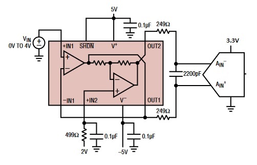
    Something like this for every cell:

    Image Courtesy: LT

    Protection diodes at output would be required to save the ADCs. Devin do share in your views.

    Regards,

    Gautam

  • I'm not sure about that specific circuit, but yes, some signal conditioning circuitry will be needed for each battery cell which scales the sensed voltage, generates the differential compliment, and sets the correct common mode.

    The easiest way to verify correct operation is by simulating the signal conditioning circuitry in TINA or a similar SPICE based circuit modeling program.  

    Protection diodes may or may not be necessary - it depends on what can come out of the signal condition circuitry.  It may be a good idea to simulate the power-up and power-down of the signal conditioning circuits to see if any transient over/under voltage conditions are produced.    

  • Devin Cottier said:
    I'm not sure about that specific circuit, but yes, some signal conditioning circuitry will be needed for each battery cell which scales the sensed voltage, generates the differential compliment, and sets the correct common mode.

    Yup... absolutely!

    Devin Cottier said:
    The easiest way to verify correct operation is by simulating the signal conditioning circuitry in TINA or a similar SPICE based circuit modeling program.