This thread has been locked.

If you have a related question, please click the "Ask a related question" button in the top right corner. The newly created question will be automatically linked to this question.

DRV8301-69M-KIT schematic to own layout

Other Parts Discussed in Thread: DRV8301-69M-KIT, MOTORWARE, DRV8301, TLV2784, TLV2781

Hi,

We have used your schematic for the DRV8301-69M-KIT, to create a smaller version with the same functionality. It is a complete copy from this schematic but with other mosfets, IRFH7004TRPBF. The layout is however competely remade. We are using two pcb:s stacked over each other. Where one is the power-PCB with mosfets and current sensing resistors and the other PCB contains all the signalling and logic hardware. But after 5 revisions and countless checks of hardware and comparision with the original design, we still have issues with getting everything to run well. We can program the F28069M with no problems and also run the laborations. Allthough here is where the problems appear. When running laboration 7c from your MotorWare library with the evaluation-kit DRV8301-69M-KIT, we have no issues and the motor is running very well. But using our own layout based on this design, the motor starts jumping very hard in the progress of identifying the motor, almost like every third phase. It can start turning but uses way to much current and gets very warm. We have made all checks against schematics and have found no error, so we are leaning towards some kind of design issue. But we have no idea of where it might appear in our hardware. The pcb:s are created using Diptrace, but we can export to numerous format and are happy to share the design with you if you have possibility to look it through. We are stranded a bit here. 

Do you have any recommendation on where to look for problems and what we can do to get forward. This is a vital project for us and the driver is intended for long term underwater autonomous vehicle as a part of one of the most critical systems on board. We love how it performs on the evaluation kit, but we have no space for this in the final mechanical design.

Best regards,

Mikael

  • I would look at your current measurement circuits. The DRV8301 EVM has some issues with current layout which makes it noisy at higher currents and PWM modulations, but it sounds like your issues are more serious than that. On the EVM we use the 3 external OPA and we amplify close to the measurement and have long traces to the ADC pin. Ideally you would amplify as close to the ADC pin as possible, and include filtering at the ADC pin. The Launchpad + BoosterPack does a better job of this.

    I would also do some testing on your measurements. Input DC values and see if the conversions are as expected. Do the offsets calculated by the labs look reasonable?
  • Thanks for the suggestions. While looking through the layout we found one small error in our design that might relate to this. In making this layout more compact we changed the TLV2781 into a package with 4 opamps, TLV2784. Leaving one opamp unconnected. We have now changed the layout so that this opamp also is terminated correctly. Hopefully this was creating the instability in the system that we saw. I will repost when we have the new layout finished, the final results.

  • Hi Mikael,

    Did you finish your new layout ?
    and how are your results ?

    I'm planning to do the same, build a smaller layout with the same schematic of the DRV8301-69M-KIT 
    Maybe you can share your design.

    Thx

  • Hi Renaud,

    The project went well, however there are a few differences in behaviour with the more compact design. Our design works much better with lower frequencies 8-15kHz, even with the smalles motors. In fact it works absolutely perfect there. Higher frequencies is almost unusable. Most likely due to disturbance in the electronics. This is also partly true with the original EVM, though not as pronounced. Increasing the resistor values for the shunts is likely to improve the results if the increased power loss can be accepted, we are also looking into rescaling the voltage sensing parts a bit. There is no final conclusion here.

    On then power side it works well up to 50A. We have a customized aluminium cooling block though.

    Unfortunately we have developed this during the last year partly for one of our customers, and it was far from an easy task. That's why we cannot share this design. However if you go for it and try yourself, I can probably help you if you have any issues. We ended up using a 6 layer design for the signalling part and one more stacked 5oz board for the power mos pcb.

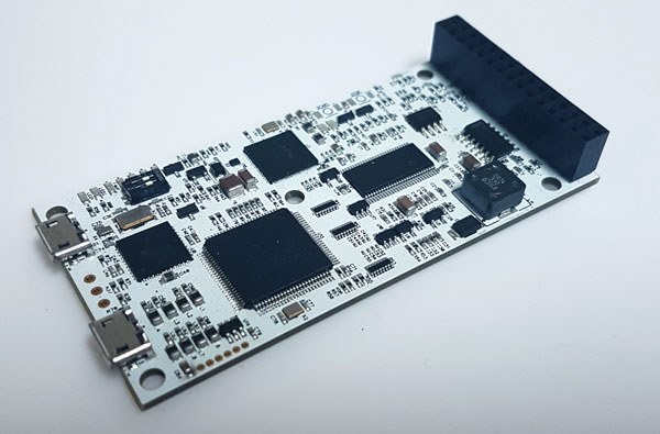
    This is a picture of the signal PCB;

    Br,

    Mikael

  • Hi Mikael,

    That's a nice PCB ! 

    I understand why you cannot share the design.
    It's good to know that it works perfectly.

    We "only" need 1.5kW so we can increase the shunt resistor.
    But first we have to make the motor work with the official EVM.

    Can you tell me what is the size of your signal and power boards ?

    Thank you.

    Renaud.


  • The two pcbs assembeled and with heatsink mounted measures 80x40x40mm.
    For that kind of power I would go for 40V system to keep the current down a bit. It will relax things. What kind of motor are you planning to use? Maybe I can help out with parameters for the EVM when you start testing.

    Br,
    Mikael
  • This sounds similar to my issues, instaspin runs my motors on boost-xl kits but I can't get any of the custom inverters I built to run, while two other ARM based FOC controllers have no issue with the same combination. Does instaspin perform any sort of signal filtering on the analogue signals? I did find on the open source controller that works with the inverter that it has a significant amount of code for filtering signals, though it's difficult to find how it is applied as there's no documentation.

    On F28069 devices would it be worth while adding additional signal filtering to try and make it more reliable across different hardware? If you're only running one motor there's plenty of resources left and the CLA.
  • voltage filtering is done inside the algorithm, based on the voltage filters (voltage filter pole frequency must be matched in user.h). Kelvin grounds are important.

    getting reliable current and voltage signals into the algorithm is critical. our Launchpad + BoosterPack references do a good job of this.

    the DRV8301-69M-KIT doesn't do as good of a job. There are long traces from the outputs of the current amplifiers to the ADC inputs on the controlCARD. On your own design you want the amplifier as close to the ADC as possible. Also follow the recommendations for standard ADC pin filtering like we do on our designs.

    see SPRUHJ1 for details on the voltage and current measurements and the associated SW variables in user.h
  • I agree that there are issues here, with our design, and even of the DRV8301-69M-KIT. Strange enough we have maybe 1/5 of the length with our traces from the voltage and current signals and still experience this. I think the lower resistance voltage dividers on the BoosterPack and the 5 times higher value of the shunt resistors are the factors that stabilize the BoostXL rather than different length of traces. We will test to rescale our boards with first the voltage dividers from the BoostXL (34.8k + 4.99k), and limit the system to 26V, and as second procedure we will increase the shunt resistors values and see if we can get a bit better results. We will also try and just rescale the DRV8301-69M-KIT voltage divider to maybe provide more current to the voltage feedback and make it less prone to disturbances. I'll get back when we have the results of this.
  • Hi again,

    As promised here is an update on the layout part of this project and some tip to you other ppl trying to customize your designs. What I found looking into the design was that the voltage sensing part of the original and our previous design was a bit sensitive to noise from the erst of the system so I went ahead and thought I could improve it a bit. I just did some rescaling on the voltage sensing part first, divided both resistors with 5 to get the same voltage output but with a little bit more current and as such less prone to disturbances. This shows a big improvement! Now we can run our small motors even at 40rpm and at 20kHz PWM. It is still not possible to run it at higher frequencies at any stability, but it is really not needed in our application. Also, the stability with 8kHz is even better than before. Since we didn't really change anything, voltage is still available up all the way to 50V. If we run smaller motors we will use double value on the shunts, 0.004 Ohms instead of 0.002. This will further increase the system sensitivity of course but at a cost of heat generation and loss of power.

    Also, a side notice, to be able to switch really fast, take into account the FET gate inductance. Use as wide and short traces as possible from the drv83 to the gates. I cannot stress this enough. Any inductance here will increase noise in the amplifier stage and the sensing part, especially at higher speeds and it will increase switching losses.
  • Hi,

    Thank you for your feedback,It's really interesting and certainly useful.
    I have a question : what is the advantage of higher PWM, since at  8kHz it's working nicely ?

  • The advantages are more acoustic than anything else. At 8kHz you can hear the switching in action. Not so much up and above 20kHz. This was important in our application. Otherwise these small BLDC:s are often more adapted to run at 8kHz PWM anyway. This is how the RC community drives them in most cases. I'd say that in every other case 8kHz is a better choice from a pure electronical point of view, since one get lower switching losses. I can't speak for TI:s algos here though, they would have to fill in regarding eventual issues using lower PWM switching speeds.