This thread has been locked.

If you have a related question, please click the "Ask a related question" button in the top right corner. The newly created question will be automatically linked to this question.

TMS320C28341: I/O pin protection

Part Number: TMS320C28341
Other Parts Discussed in Thread: TMS320F2808,

Hello,

I am designing lightning protection circuitry around the I/O pins for the TMS320F2808 processor. I couldn’t find this in the input menu, so I chose one close. The test waveforms to be injected on the input connector pins conform to the airborne standard RTCA/DO160G Section 22, waveforms 3/3 and 4/1 at level 3.

My approach is to augment the internal clamp diodes with external schottky clamps, as illustrated below:


My question is; what is the nominal forward drop across the internal clamp diodes for the GPIO I/O pins for this processor?

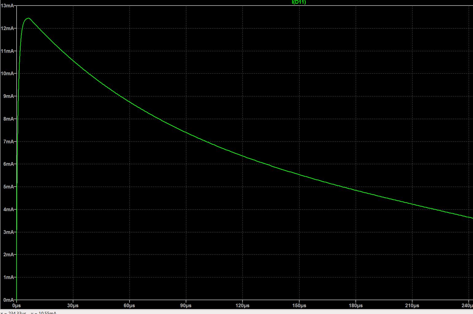
I have simulated this with a relatively high drop schottky, the MBR21011CT, but I am just guessing.

Also, I assume that the maximum spec for input clamp current (±20ma) refers to the maximum current through the internal clamp diodes.

Thanks,

Larry Richardson

  • Larry,
    I am unable to see the image. Could you attach it as a file? On a different note, the "Part number" on the title is TMS320C28341, but the body of the post refers to TMS320F2808. Which is the correct part number?
  • Larry,

    Can't see the image and I'm not personally familiar with the RTCA standard you mention but I assume this is protection for pins which could see a system level ESD event cause high pin voltages.

    Nominally the clamp diodes are about 0.7v, but they can begin conducting weakly at as little as 0.3v (will vary by device and temperature).  The 0.3v level is more of a consideration to avoid for continuous over-voltage conditions, however we don't have a specified limit for when the clamp diodes turn on.

    The 20mA maximum is for all components in the circuit, this shouldn't be exceeded whether it is through the ESD clamp diode or the Output buffer.  The approach of external schottky's is good, as well as a series resistor to the F2808 device to limit the current to below 20mA.  

    You might check out the IBIS models as well, you can find them here:

    Best regards,

    Jason

  • Jason,

    This reply resolves my issue. I already have 50 ohms in series with the GPIO pins, but can't go much higher because of rise/fall time requirements downstream. The DO160G requires a 300V sustained transient to be applied to the input pin, which results in some pretty hefty currents internally. I have two parallel low-drop schottkys on the two pins of concern, and am modeling the internal clamps with higher drop diodes. I just wanted to make sure the internals were indeed higher drop than my externals.

    I have attached an image of my LTSpice simulation since it didn't make it originally.

    Thanks,

    Larry Richardson

  • Larry,

    Thanks for the follow up, glad it looks like you are on the way to a solution.  Have you looked at putting the series resistor instead at a point in between your two Schottkys and the TMS320 pin?  This would help force the current preferentially through the external Schottkys vs. the TMS320 internal protection.  There are probably other considerations as well, just mentioning it.

    Best regards,

    Jason

  • Jason,
    Thanks. I will try that. It should not effect anything else downstream.
    Larry
  •  Before 50 ohm move.

     After move

    Thanks. I was considering putting yet another pair of those large package Schottkys in, and my pcb guy would have killed me. ;-)

    Larry