This thread has been locked.

If you have a related question, please click the "Ask a related question" button in the top right corner. The newly created question will be automatically linked to this question.

TMS320F28075: ADC sampling result has 2nd harmonic while ADC analog input hasn't

Part Number: TMS320F28075
Other Parts Discussed in Thread: C2000WARE

Hi

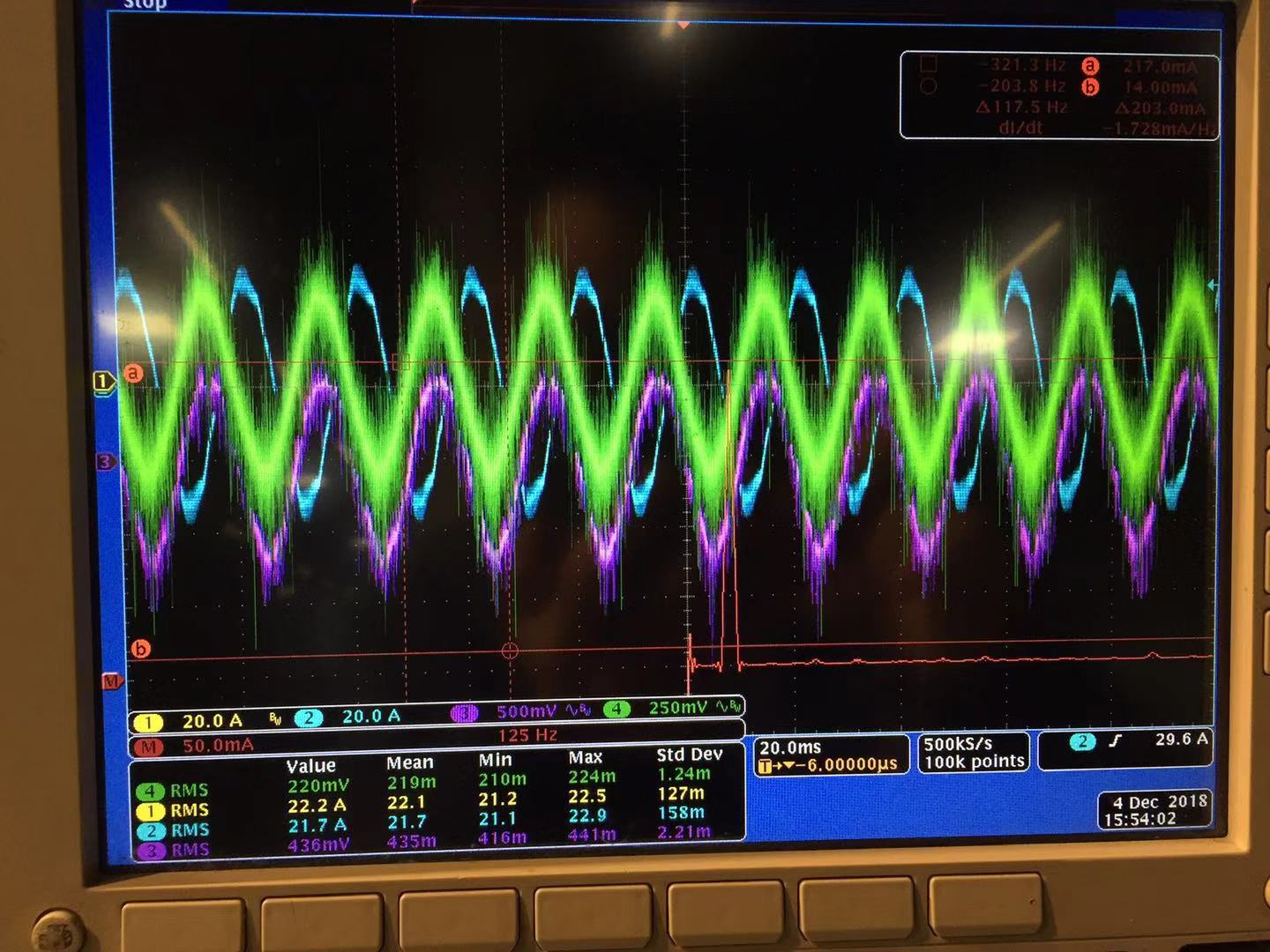
My customer use TMS320F28075 ADC to sample three-phase electric power.

As you see, the green wave is voltage input to ADC. Fundamental is 50Hz, almost hasn't 100Hz harmonic. 

The purple is the converted wave from digital ADC sampling result. 100Hz harmonic become heavy. 

Analog input hasn't 100Hz 2nd harmonic, why the ADC sampling result has so heavy 2nd harmonic? Thanks.

  • Hi Daniel,

    How is the sampled waveform reconstructed?

    Do you have a spectrum plot of both the input waveform and the reconstructed waveform?

    What do the signal conditioning circuits look like in this case?: What is the driving buffer and topology, if any? What is the resistive impedance on the input? How much capacitance is on the input? What is the S+H duration? What is the sample rate?

    If you want to test the performance of the ADC from a THD/SNR perspective I'd highly recommend using the following EVM as a signal source: http://www.ti.com/tool/PSIEVM
  • Hi,

    acqps =  14

    Test signal is:ADC_IR,ADC_IS

  • Hi Daniel,

    I'm not sure your schematic snippet answers the question of what the signal conditioning circuits look like. The question is what do the signal conditioning circuits for ADC_IR and ADC_IS look like - specifically what amplifier (if any) is driving the input and what passives (R and C) are between the drive stage and the input. You could also have something like a current sense resistor, a voltage divider, or some other type of sensor.

    Based on your code snippet, you are using S+H duration (S+H = 15 SYSCLKs = 15*8.333ns = 125ns)? This is pretty close to the minimum S+H duration of 100ns, so I'd expect the input to be driven by a high-bandwidth op amp with a capacitor of about 20*Ch = 20*16.5pF = 330pF and a resistor that is around 10-100 ohms (depending on the op-amp).

    Are the VREFHI inputs directly connected to VDDA/VDDIO? Any noise on this input will directly couple to the output, so this could definitely be the source of some distortion.

    Overall I still think the best debug would be to examine the spectrum:
    -Of the input directly
    -Of the sampled input reconstructed via the output path
    -Of the output path when creating an ideal waveform (ideal digital codes to the DAC/ePWM)
    -Of an ideal analog input sampled and then reconstructed via the output path

    This should give you a good idea of how much distortion is introduced at each stage (input, sampling, reconstruction) so that you can target debug efforts appropriately.
  • Hi Devin,

    Thanks for your advice.

    Connect VREFHI、VDDA、VDDIO to 3.3V together, do you have recommended circuit about this?

    We judge the signal changed after ADC_IR and ADC conversion. It should be independent with ADC_IR amplifier.

    Besides, we will enlarge sampling time to test it again.
  • Hi Daniel,

    For the VREFHI driving circuit you can refer to Launchpad or ControlCard schematic in C2000ware.  We also have a section in the TRM describing the circuit:

    The ADC input itself is not high impedance; it very much matters what you are using to drive it.  It is possible that if the driver impedance is too high or the bandwidth is too low you will not be able to feasibly drive the ADC input with any length S+H window. 

  • Hi Devin,

    Sorry for we need some more time to do the test. Will give you update when we test it later.
  • Hi Daniel,

    No problem.  If this thread locks, use the 'ask a related question' button to continue the discussion.